General, quoting & support.
Add: Building E, No.58, Nanchang Road, Xixiang , Baoan District Shenzhen City, Guangdong, China
Tel : 0755-27348887
Fax : 0755-27349876
E-mail : svc@pcbastore.com

Beyond FR-4: PCB Materials for Future Electronics
PCBA Store / 2026-08-25
Contents [hide]
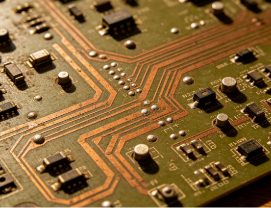
Standard FR-4 still handles many basic circuit board needs. However, faster data speeds and higher power densities are shifting design choices. Smaller product assemblies also force engineers to rethink their options. Choosing the correct base layer today involves careful comparisons. Designers must look closely at signal loss and heat transfer. Mechanical behavior, manufacturing limits, and overall production costs also play major roles.
Why Electronics Are Moving Beyond Standard FR-4
An fr4 pcb remains a highly practical option for everyday consumer devices. It works very well in industrial controls and communication terminals. This substrate provides an excellent balance of electrical insulation and tough mechanical strength. It is widely available and keeps fabrication costs low. Furthermore, its well-known manufacturing process helps teams easily move prototypes straight into mass production.
Problems usually start when operating conditions exceed the limits of a standard FR-4 grade. For instance, fast digital signals might experience severe insertion loss. Tightly packed power components often generate intense local heat. This extra heat can easily shorten the working life of the device. Additionally, repeated soldering cycles and constant temperature changes put heavy stress on internal vias. These thermal shifts also strain delicate copper traces and internal laminate layers.
High-Tg FR-4 certainly extends the safe operating range of a board. Yet, the glass transition temperature (Tg) alone never tells the whole story about material performance. A smart designer must also check the decomposition temperature and the coefficient of thermal expansion. Moisture absorption rates, the dielectric constant, and the dissipation factor need careful review too. Furthermore, engineers should check the time to delamination. Simply having a high Tg value does not magically make a substrate right for sensitive microwave signals or heavy thermal loads.
Which Advanced PCB Materials Address These Limits?
Each material family solves a different engineering problem. Replacing FR-4 without identifying that problem can increase cost while providing little practical benefit.
PCB material | Main advantage | Typical applications | Main design concern |
High-Tg FR-4 | Better thermal robustness | Industrial controls, automotive systems | Still has signal-loss limits |
Low-loss laminate | Reduced high-frequency loss | Servers, high-speed networks, 5G equipment | Stackup and copper profile |
PTFE-based laminate | Stable RF performance | Radar, antennas, microwave circuits | Specialized processing |
Aluminum-core material | Direct thermal path | LED lighting, power converters | Limited multilayer flexibility |
Polyimide | Flexibility and heat resistance | Flex and rigid-flex PCB designs | Bend and dimensional control |
Ceramic substrate | Heat transfer and insulation | Power modules, EV systems | Brittleness and higher cost |
Low-Loss Laminates Protect High-Speed Signals
Low-loss laminates become highly valuable under strict electrical conditions. They are necessary when long copper traces or fast edge rates push past normal limits. High operating frequencies also make standard FR-4 signal drops completely unacceptable. These specialized laminates feature a tightly controlled dielectric constant. They also offer a very low dissipation factor. Together, these traits successfully maintain proper signal strength and precise timing across the entire board.
Picking the right substrate cannot rely entirely on just one Dk or Df number. Many subtle factors influence the actual data channel performance. The specific test method and test frequency matter greatly. Resin mixtures, glass weave styles, and copper surface roughness also play huge roles. Using low-profile copper effectively reduces conductor signal drops. Meanwhile, highly stable dielectric properties allow engineers to model trace impedance and signal travel speeds with much better accuracy.
PTFE Supports RF and Microwave Performance
PTFE-based laminates deliver extremely low dielectric loss. They also provide incredibly stable electrical behavior at demanding microwave frequencies. These unique traits make them perfect for complex antennas and sensitive radar sensors. They are equally useful for satellite communication gear, powerful RF amplifiers, and precision measurement tools.
Manufacturing these boards demands much tighter control than standard FR-4 production. Mechanical drilling and hole wall preparation need highly specific machine settings. Copper adhesion, dimensional scaling, and multilayer pressing also require custom parameters. Sometimes, engineers use a clever hybrid layer stackup. This method places expensive PTFE only inside the critical RF sections. It then keeps cheaper FR-4 layers everywhere else. This smart tactic definitely controls overall costs. However, it introduces tricky bonding challenges and mismatched expansion rates. Teams must carefully review these physical risks before starting the fabrication process.
Metal-Core Materials Move Heat Away from Components
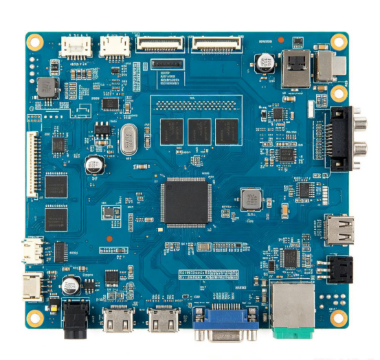
An aluminum-core PCB uses a thermally conductive dielectric between the circuit copper and metal base. Heat travels through this structure toward a heat sink or enclosure, reducing the temperature around LEDs, power semiconductors, and other high-load components.
Thermal conductivity is only one part of the decision. Dielectric thickness, breakdown voltage, copper weight, component layout, interface material, and final heat-sink design determine the complete thermal path. A high nominal conductivity cannot compensate for poor contact with the enclosure or an undersized heat sink.
Metal-core boards are common in LED lighting, motor drives, charging equipment, and power conversion. They generally cost less than ceramic solutions, but their electrical isolation and temperature capability depend heavily on the dielectric layer.
Polyimide Enables Flexible and Rigid-Flex Designs
Polyimide combines electrical insulation with flexibility and thermal stability. It supports compact interconnections in cameras, medical devices, robotics, aerospace systems, wearables, and products where separate rigid boards would otherwise require cables and connectors.
A flexible circuit still needs a defined mechanical operating condition. The designer should distinguish between a circuit bent once during installation and one exposed to continuous movement. Bend radius, copper type, conductor direction, coverlay openings, stiffeners, and component placement all affect fatigue life. Flex-circuit material suppliers also identify dimensional stability and controlled adhesion as important requirements for fine-feature and multilayer construction.
Rigid-flex PCB designs can reduce connector count and assembly space, but they require the mechanical and electrical stackups to be developed together. Treating the flex section as a late replacement for a cable often creates avoidable reliability problems.
Why Prepreg Materials Affect the Entire Stackup
Prepreg materials bond the cores and copper layers in a multilayer PCB, but their role extends beyond adhesion. After lamination, prepreg forms the dielectric spacing that influences impedance, board thickness, insulation, and mechanical stability.
Resin content and flow determine whether etched copper areas fill correctly during pressing. Too little resin may leave voids or weak bonding around dense copper patterns. Excessive resin movement can change dielectric thickness and affect impedance. Glass style also matters because signals passing through different proportions of glass and resin may see different effective dielectric properties.
The laminate, prepreg, copper profile, and press cycle should therefore be approved as one material system. Substituting a “similar” prepreg without reviewing cured thickness, Dk, Df, resin content, and flow behavior can change both electrical performance and production yield.

Material Choice Must Include PCB and PCBA Processes
Advanced PCB materials affect drilling, desmear, plating, lamination, routing, storage, and surface preparation. They may also change minimum order quantities, panel utilization, procurement time, and scrap risk. Material availability should be confirmed before a design is released for production.
PCBA conditions add another layer of risk. Lead-free reflow, heavy components, large BGAs, and repeated thermal cycles can expose weaknesses in the substrate or stackup. The solder profile, moisture controls, surface finish, stencil, inspection method, and functional test plan should be reviewed with the bare PCB construction.
PCBA Store supports PCB fabrication with FR-4, PI, aluminum, ceramic, and PTFE options, followed by SMT, through-hole, or mixed-technology PCB assembly. Available inspection and testing processes include AOI, X-ray inspection for packages such as BGA and QFN, ICT, and functional testing. This combined review helps connect material selection with actual assembly conditions.
Choose Material by Risk, Not by Trend
The right next-generation material is not always the material with the highest published performance. It is the option that satisfies the electrical, thermal, mechanical, and environmental requirements with an acceptable manufacturing window.
Before requesting a quotation, define the operating frequency, voltage, current, heat load, layer count, impedance targets, board dimensions, copper weight, reflow exposure, expected service life, and production volume. Also state whether material substitutions are permitted. These inputs allow the fabricator to identify risks before prototype production.
Ready to review a new stackup? Use the PCBA Store online quote system for standard requirements, or upload your PCB files, stackup, BOM, and assembly documents for a detailed manufacturing quotation.
FAQ
Is high-Tg FR-4 an advanced PCB material?
High-Tg FR-4 offers better resistance to thermal expansion and repeated heat exposure than standard grades. It is useful for demanding multilayer and lead-free assemblies, but it does not automatically provide low RF loss or high thermal conductivity.
When should a ceramic PCB replace an aluminum PCB?
A ceramic PCB becomes relevant when the design requires stronger electrical insulation, higher temperature capability, or a more direct thermal path. Aluminum PCB materials often remain more economical for LED and general power applications.
Which PCB material is suitable for high-frequency circuits?
PTFE-based laminates and low-loss thermoset materials are common choices. The final selection should use frequency-specific Dk and Df data, expected insertion loss, copper roughness, impedance targets, and the fabricator’s processing capability.
Can FR-4 and RF materials be used in one PCB?
Yes. A hybrid multilayer PCB can combine RF material with FR-4-compatible layers to control cost. Lamination compatibility, bonding, thickness tolerance, drilling behavior, and thermal expansion must be validated before production.
What information is needed to quote a special-material PCB?
Provide Gerber or ODB++ data, drill files, stackup, material grade, board thickness, copper weight, impedance requirements, surface finish, quantity, and applicable test criteria. PCBA quotations should also include the BOM, centroid file, and assembly drawings.
Previous article:Top PCB Assembly Defects and How to Prevent Them During Production



