Add: Building E, No.58, Nanchang Road, Xixiang , Baoan District Shenzhen City, Guangdong, China
Tel : 0755-27348887
Fax : 0755-27349876
E-mail : svc@pcbastore.com

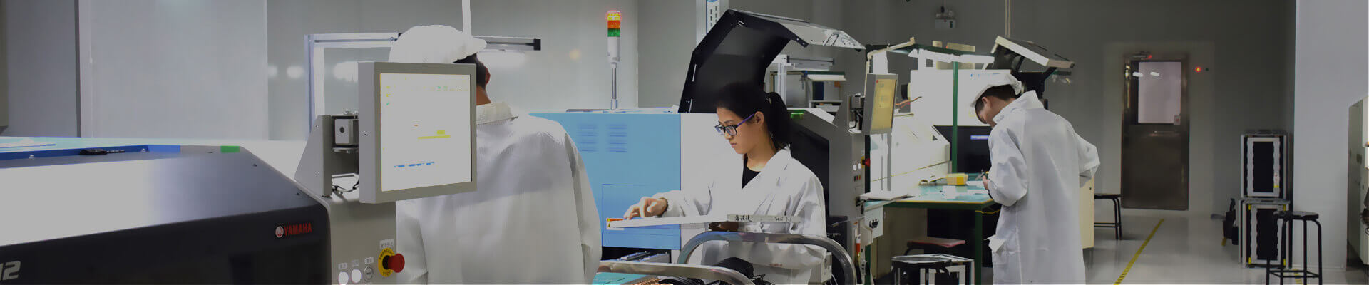
We thought it necessary to talk about this topic due to high amount of inquiries regarding the assembly process.The PCB assembly process is a simple one, consisting of several automated and manual steps. With each step of the process, a board manufacturer has both manual and automated options from which to choose. The following is intended only as an introduction to the pcb assembly processes as a training aid for customers and friends of PCBAStore. Some depict specific processes used by PCBAStore and may not reflect practices used by other manufacturers. Although this article is elementary, it allows our customers to gain a bit of a better perspective on the process of the printed circuit board assembly.
Step2 Preparing Film
Step4 Innerlayer Imaging
Step6 AOI
Step8 Drilling
Step10 Outerlayer Imaging
Step12 Etching outerlayer
Printed Circuit Board Assembly (PCBA) is the finalized board that is obtained after all the components have been mounted on the printed circuit board(PCB). These components may include resistors, capacitors, integrated circuits (ICs), and others depending on the application of the electronic device. In order to ensure a mechanical connection between the board and components, the PCBA for smart devices must undergo reflow furnace heating.
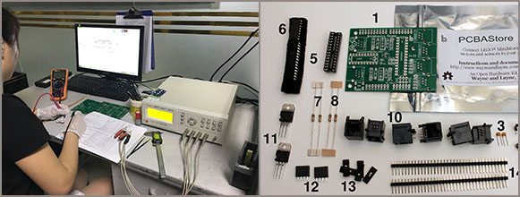
Given below are a list of electronics and associated consumables that are necessary for printed circuit board assembly:
• Printed Circuit Board (PCB)
• Electrical componentssuch as resistors.
• Soldering materials such as wire, preforms, bar, flux and paste.
• Soldering equipment such as wave soldering machine, surface mounter, SMT-Stencil, soldering fixture and testing tools etc.
A Printed Circuit Board (PCB) is the focus of assembly before, that is the base for wiring and supporting surface-mounted, socketed components in electronics. In circuits where there is a need for find conductive traces (such as computer systems), these PCBs are made through the photolithographic process. This is similar to the way conductive paths are made for processors just that it is on a much larger scale. The three primary PCB types include:
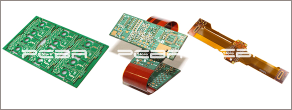
• Rigid PCB: The most common type of PCB base is a rigid one. The solid core of a rigid PCB gives the board rigidity and thickness. These inflexible PCB bases consist of a few different materials. The most common is fiberglass, otherwise designated as "FR4. " Less expensive PCBs are made with materials like epoxies, PTFE or ceramic, though these are less durable than FR4
• Flexible PCB: Flexible PCBs offer a bit more pliability than their more rigid counterparts. The material of these PCBs tends to be a bendable, high-temperature plastic like Kapton.
• Metal Core PCB: These boards are yet another alternative to the typical FR4 board. Made with a metal core just like copper or aluminum based etc., these boards tend to spread heat more efficiently than others. This helps dissipate heat and protect more heat-sensitive board components.
The PCB designer has prepared his layout on a Computer Aided Design or CAD system. Most PCB assembly companies need the design file of the PCB to start out, along with any other design notes and specific requirements. This is so the assembly company can check the PCB file for any issues that may affect the PCB's functionality or manufacturability. This is a design for manufacturability check, or DFM check, for short.
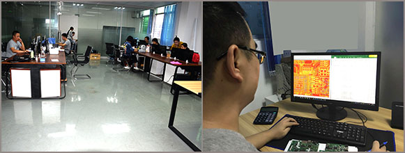
The DFM check looks at all the design specifications of a PCB. Specifically, this check looks for any missing, redundant or potentially problematic features. Any of these issues may severely and negatively influence the functionality of the final project. For example, one common PCB design flaw is leaving too little spacing between PCB components. This can result in shorts and other malfunctions.
By identifying potential problems before manufacturing begins, DFM checks can cut manufacturing costs and eliminate unforeseen expenses. This is because these checks cut down on the number of scrapped boards. As part of our commitment to quality at a low cost, DFM checks come standard with every PCBAStore project order.
PCBAStore Verifying all incoming materials and handling quality problems before subsequent SMT assembly begins. Our IQC position will check following issues of incoming materials if they comply with our strict requirements.
• model number and quantities according to BOM list
• shape (deformation, broken pin, oxidation etc), particularly for IC or other complex components
• sample test of incoming materials by tools such as test frame, multimeter etc.
• If above defect or discrepancy occurs, we will return full incoming materials to supplier or customer.
This process is used by Process Engineers to program our Automatic Assembly Equipment (Printing, Pick and Place Machines, Soldering, AOI Inspection, X-Ray Machine). PCBAStore has a proprietary, automated process that lets us set-up machines in hours rather than the days it takes other shops. After programming is complete, we can start the next step
Prior to the addition of the components to a board, solder paste needs to be added to those areas of the board where solder is required. This process is like screen-printing a shirt, except instead of a mask, a thin, stainless-steel stencil is placed over the PCB. This allows technician to apply solder paste only to certain pads of the would-be PCB. These pads are where components will sit in the finished PCB.
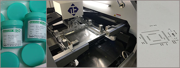
The solder paste itself is a greyish substance consisting of tiny balls of metal, also known as solder. The composition of these tiny metal balls is 96.5% tin, 3% silver and 0.5% copper for RoHS-complaint and 63% tin, 37% lead for leaded process. The solder paste mixes solder with a flux, which is a chemical designed help the solder melt and bond to a surface. Solder paste appears as a grey paste and must be applied to the board at exactly the right places and in precisely the right amounts.
In our automatic printing machine, a mechanical fixture holds the PCB and solder stencil in place. An applicator then places solder paste on the intended areas in precise amounts. The machine then spreads the paste across the stencil, applying it evenly to every open area. After removing the stencil, the solder paste remains in the intended locations. Solder paste printing is the most important part of quality control in PCB assembly process. PCBAStore's advanced machine and excellent engineer is the guarantee for this.
After applying the solder paste to the PCB board and passing the automatic inspection, the assembly process moves on to the pick and place machine(SMT Mounter).
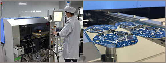
This robotic device places surface mount components, or SMDs, on a prepared PCB. SMDs account for most non-connector components on PCBs today. The device starts the pick and place process by picking up a PCB board with a vacuum grip and moving it to the pick and place station. The robot then orients the PCB at the station and begins applying the SMDs to the PCB surface. These components are placed on top of the soldering paste in preprogrammed locations.
In some assembly processes, the pick and place machines add small dots of glue to secure the components to the board. However this is normally done only if the board is to be wave soldered. The disadvantage of the process is that any repair is made far more difficult by the presence of the glue, although some glues are designed to degrade during the soldering process.
if the board is to be wave soldered. The disadvantage of the process is that any repair is made far more difficult by the presence of the glue, although some glues are designed to degrade during the soldering process.
The joining of components to the PCB is usually done by machine, but in special cases, place is done by hand.
These SMDs are then soldered on to the surface of the board in the next step of the assembly process.
Once the components are placed on the boards, each piece is sent through our 10-zone reflow machines. This means the solder paste needs to solidify, adhering components to the board. PCB assembly accomplishes this through a process called "reflow. "
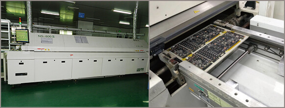
After the pick and place process concludes, the PCB board is transferred to a conveyor belt. This conveyor belt moves through a large reflow oven, which is somewhat like a commercial pizza oven. This oven consists of a series of heaters which gradually heat the board to temperatures around 250 degrees Celsius, or 480 degrees Fahrenheit(Sn/Pb paste for 240 degrees, Sn/Ag/Cu paste for 260 degrees). This is hot enough to melt the solder in the solder paste.
Many PCB assemblies will need special consideration during the reflow process. Most notable of these are two-sided boards. Typically, the two-sided board assembly process involves stenciling and reflowing each side separately. First, the side with the fewest and smallest parts is stenciled, placed and reflowed, followed by the other side.
Once the surface mount components are soldered in place after the reflow process, the board can be checked whether the quality is acceptable. Often, movement during the reflow process will result in poor connection quality or a complete lack of a connection. Shorts are also a common side effect of this movement, as misplaced components can sometimes connect portions of the circuit that should not connect.
Checking for these errors and misalignments can involve one of several different inspection methods. The most common of these inspection methods include the following:
• Manual Checks: For smaller batches, an in-person visual inspection by a QC Inspector is an effective method to ensure the quality of a PCB after the reflow process. However, this method becomes increasingly impractical and inaccurate as the number of inspected boards increases. Manual inspection is not an option for surface mount boards employing a hundred or more components.
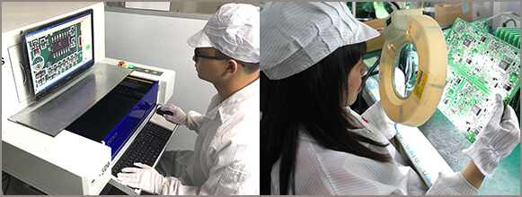
• Automatic Optical Inspection(AOI): AOI is a more appropriate inspection method for larger batches of PCBs. An AOI machine, uses a series of high-powered cameras to "see" PCBs. These cameras are arranged at different angles to view solder connections. Different quality solder connections reflect light in different ways, allowing the AOI to recognize a lower-quality solder. The AOI does this at a very high speed, allowing it to process a high quantity of PCBs in a relatively short time.
• Automated X-ray inspection(AXI): Yet another method of inspection involves x-rays. This is a less common inspection method — it's used most often for more BGA board.As BGA connections are not visible the only alternative is to use a low level X-ray inspection. AXI is able to find faults such as opens, shorts, insufficient solder, excessive solder, missing electrical parts, and mis-aligned components. Defects are detected and repaired within short debug time. These inspection systems are more costly than ordinary optical systems, but they are able to check all the connections, even those underneath the chip package.The X-ray also allows a viewer to see through layers and visualize lower layers to identify any potentially hidden problems.
The fate of a malfunctioning board depends on the assembly company's standards. Malfunctioning boards are either sent back to be cleared and reworked, or they're scrapped. PCBAStore's quality standards are based on the industry standard IPC-A-610 improved.
Depending on the type of board under assembly, the board may include a variety of components beyond the usual SMDs. These include plated through-hole (PTH) components.
A plated through-hole is a hole in the PCB that's plated all the way through the board. PCB components use these holes to pass a signal from one side of the board to the other. In this case, soldering paste won't do any good, as the paste will run straight through the hole without a chance to adhere.
Instead of soldering paste, then, PTH components require another soldering method. The options available include manual soldering and wave soldering.
• Manual Soldering: Manual through-hole insertion is a straightforward process. Typically, one person at a single station will be tasked with inserting one component into a designated PTH. Once they're finished, the board is transferred to the next station, where another person is working on inserting a different component. The cycle continues for each PTH that needs to be outfitted. This can be a lengthy process, depending on how many PTH components need to be inserted. Most companies specifically try to avoid designing with PTH components for this very purpose, but PTH components are still common among PCB designs. Mannual soldering is offen used in the assembly of prototypes and small orders.
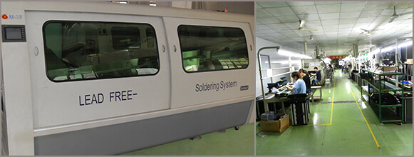
• Wave Soldering: Wave soldering is the automated version of manual soldering, but involves a very different process. Once the PTH component is put in place, the board is put on yet another conveyor belt. This time, the conveyor belt runs through a specialized oven where a wave of molten solder washes over the bottom of the board. This solders all of the pins on the bottom of the board at once.
This kind of soldering is nearly impossible for double-sided PCBs, as soldering an entire side of the PCB would render any delicate electronic components useless.
After this soldering process is finished, the boards can run through the previous steps if the PCB needs additional parts added or another side assembled. Wave Soldering is offen used in the assembly of high-volume orders.
Some completed Printed Circuit Board Assemblies have a conformal coating. It's usually depends on the customer's product requirements.
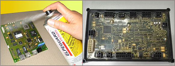
Similar to a thick paint, a conformal coating is a clear or opaque protective covering that seals the components and circuits of a PCBA. It prevents dust, chemicals, or moisture from attacking the finished PCBA.
Because the components become sealed, conformal coating makes rework or repair difficult. Conformal coating is only applied after all testing and rework is finished.
After the soldering and conformal coating step of the PCB assembly process is finished, a final inspection will test the PCB for its functionality by our Quality Assurance team. This inspection is known as a "functional test". The test software and tools are usually provided by the customer, PCBAStore can also make fixtures according to customer requirements. The test puts the PCB through its paces, simulating the normal circumstances in which the PCB will operate. Power and simulated signals run through the PCB in this test while testers monitor the PCB's electrical characteristics.
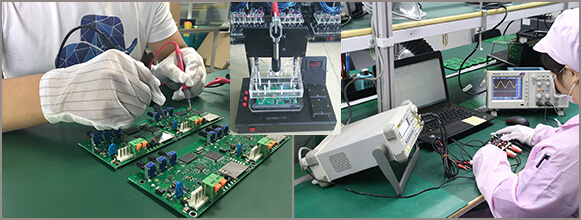
If any of these characteristics, including voltage, current or signal output, show unacceptable fluctuation or hit peaks outside of a predetermined range, the PCB fails the test. The failed PCB can then be rework or scrapped, according to the industry standards or special standards for advance agreements with our customers.
Testing is the final and most important step in the board assembly process, as it determines the success or failure of the process. This testing is also the reason why regular testing and inspection throughout the assembly process is so important.
Suffice it to say, the manufacturing process can be a filthy one. Soldering paste leaves behind some amount of flux, while human handling can transfer oils and dirt from fingers and clothing to the surface of the board. Once all is said and done, the results can look a little dingy, which is both an aesthetic and a practical issue.
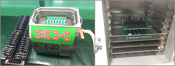
A stainless-steel, high-pressure washing apparatus using deionized water is the best tool for removing residue from PCBs. Washing PCBs in deionized water poses no threat to the device. This is because it's the ions in regular water that do damage to a circuit, not the water itself. Deionized water, therefore, is harmless to PCBs as they undergo a wash cycle.
After washing, a quick drying cycle with compressed air leaves the finished PCBs ready for packaging and shipment.
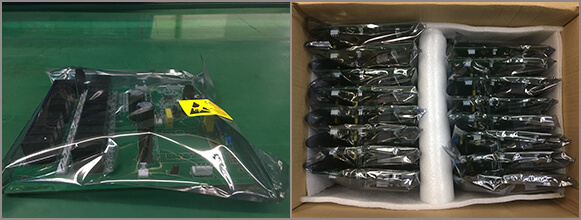
All assembled boards are packaged in anti-static packaging and shipped FedEx or UPS. Any unused components are returned in accordance with customer instructions. Additionally, customers are notified via email when their packages ships.
PCBAStore is the leading turn key printed ciruit board assembly solutions provider. We can cover each one of your PCB requirements, from parts sourcing to PCB assembly. We'll help you with each step of the way and provide you with comprehensive expertise and quality assurance. We have big capabilities for SMT/SMD assembly (also including Flexible Printed Circuit), through-hole and mixed technology PCB assemblies. BGA down to 0.25mm pitch, 0201 parts placements and leadless devices assembly can also be available. High speed advanced YAMAHA SMT mounters can well support your strict requirements of PCB assembly, whatever in relation to network, communication, health care, medical, musical instrument application. In terms of pass rate, we have done 99.9%.Our PCB assembly services meet the highest quality benchmarks and follow IPC Class 2/3, RoHS and ISO 9001:2015-certificitation standards.
To learn more about what PCBAStore can do for you and your next PCB assembly project, take a look at our PCB assembly services and get a free online quote now!
 Follow Us:


Contact Us: Please send Gerbers to svc@pcbastore.com for quotation
© pcbastore.com,All Rights
