Add: Building E, No.58, Nanchang Road, Xixiang , Baoan District Shenzhen City, Guangdong, China
Tel : 0755-27348887
Fax : 0755-27349876
E-mail : svc@pcbastore.com

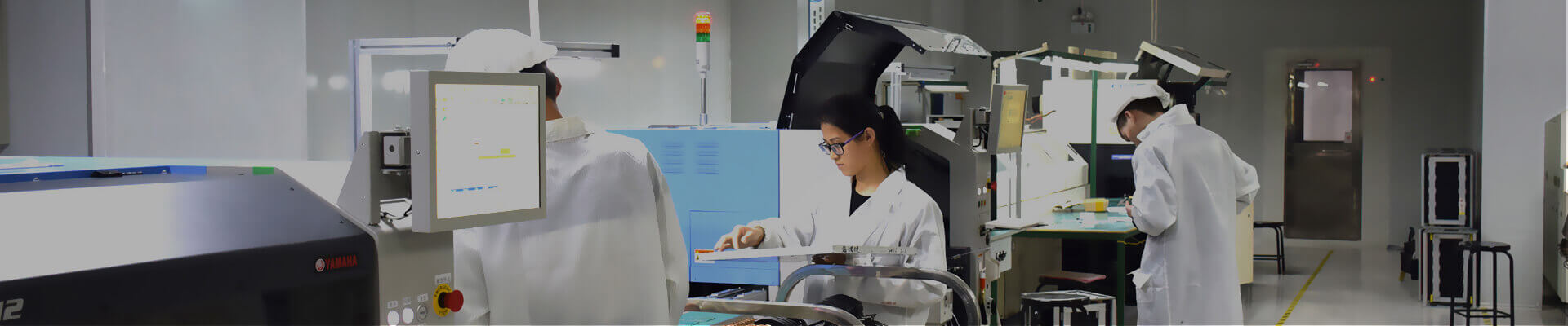
At PCBAStore we handle the PCB manufacturing process for customers from start to finish, but we believe it's important that our customers understand what we do - this ensures that your design specifications better serve your interests. General understanding of the PCB manufacturing process prevents unnecessary errors from getting transmitted during the design stage. The following is intended only as an introduction to the production processes used in building a circuit board and as a training aid for customers and friends of PCBAStore. Many of the process descriptions used here are very generic in nature. Some depict specific processes used by PCBAStore and may not reflect practices used by other manufacturers.
Step2 Preparing Film
Step4 Innerlayer Imaging
Step6 AOI
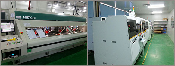
Step8 Drilling printed circuit
Step10 Image the outer layers
Step12 Etching outerlayer
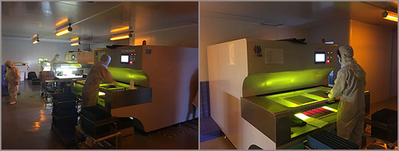
Step14 Solder Mask
Step16 Silk Screen
Step18 Final E-T
Step20 Packing & Shipping

Step1 DFM
Step3 Cutting Material
Step5 Etching innerlayer
Step7 Lamination
Step9 PTH
Step11 Plating
Step13 AOI/E-T Outerlayer
Step15 Surface Treatment
Step17 Profiling
Step19 FQC
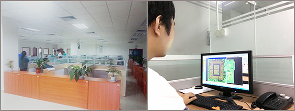
The PCB designer has prepared his layout on a Computer Aided Design or CAD system.Each CAD system uses its own internal data format, so the PCB industry has developed a standard output format to transfer the layout data to the manufacturer. This is Extended Gerber or RS274X. The Gerber files define the copper tracking layers as well as the soldermasks and component notations. First we check that data meets our manufacturing requirements. We check the track widths, the space between tracks, the pads around the holes, the smallest hole size etc. The engineer can also check and measure individual areas where he wishes. That's called a Design for Manufacture (DFM) check. Once the data is verified as good he will output all the tool files needed to drive the machines that will make and test the PCB.
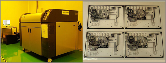
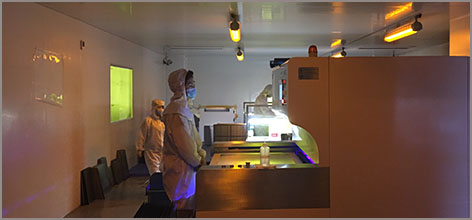
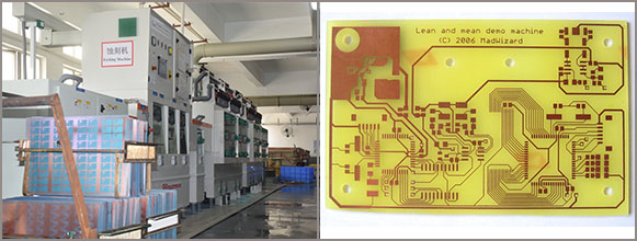
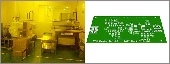
We use laser photoplotters in a temperature and humidity-controlled darkroom to make the films we will use later to image the PCBs. The photoplotter takes the board data and converts it into a pixel image. A laser writes this onto the film. The exposed film is automatically developed and unloaded for the operator. The films are ready now for the PCB fabrication process.
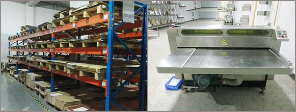
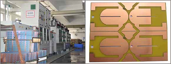
The copper-clad panels along with the drill entry material & a back-up-board are cut to size for down stream process. The standard panel is an epoxy resin and glass-fibre core with copper foil pre-bonded onto each side.
To produce the inner layers of our multilayer PCB, we start with a panel of laminate. Panels are coated by double films and then exposed to a high intensity ultraviolet light source coming. Clear areas allow light to pass through and polymerize (harden) the film resist thus creating an image of the circuit pattern –similar to a negative and a photograph.Then the copper is chemically removed from the core in all areas not covered by the dry-film resist. This creates the copper pattern that matches the film pattern.The core laminate surface is exposed in areas where copper was etched away.
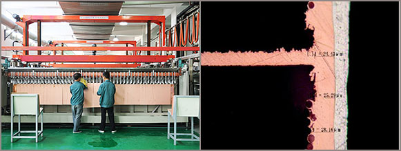
We remove the unwanted copper using a powerful alkaline solution to dissolve (or etch away) the exposed copper from the inner layer. The process is carefully controlled to ensure that the finished conductor widths are exactly as designed. But designers should be aware that thicker copper foils need wider spaces between the tracks. The operator checks carefully that all the unwanted copper has been etched away.
The inner core of our multilayer is now complete. Next we punch the registration holes we will use to align the inner layers to the outer layers. The operator loads the core into the optical punch which lines up the registration targets in the copper pattern and punches the registration holes. We won’t be able to correct any mistakes on the inner layers once we have assembled the multilayer so we now give the panel a complete machine inspection.The automatic optical inspection system scans the board in broad strips and compares it with the digital image generated from the original design data. Any errors are displayed on screen. If allowed and practical, some repairs can be made at this point. Information on defects is shared with the appropriate departments to correct any process problems.
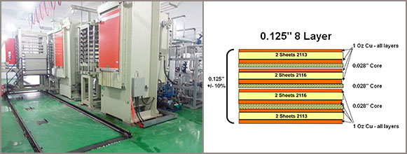
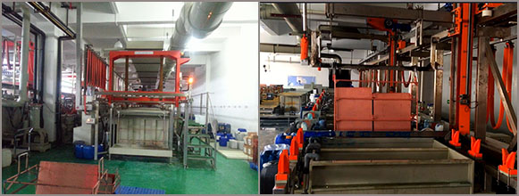
Inner layer core, copper foil and prepreg are bonded together under heat and pressure, sometimes in a vacuum, during the lamination process. The result is a panel with several layers of copper inside as well as the foil on the outside.
Now we drill the holes for leaded components and the via holes that link the copper layers together. First we use an X-ray drill to locate targets in the copper of the inner layers. The machine drills registration holes to ensure that we will drill precisely through the centre of the inner layer pads. Drilled hole sizes are usually 5 mils larger than finished plated through hole sizes to allow for the copper plating process.
The first step in the plating process is the chemical deposition of a very thin layer of copper on the hole walls.This creates a metallic base for electroplating copper into the holes and onto the surface.
The same imaging process used on the inner layers is used for the outer layers.
Next electroplate the boards with 25 microns of copper through the hole and an additional 25 – 30 microns on the tracks and pads, depending on the required final finish for the panel.
We have now plated the panel with copper that is covered with a thin layer of tin as an etch resist. We will remove the unwanted copper foil from the surface.Then the tin is chemically removed leaving behind a bare copper and laminate panel. The surface pads, traces and plated through holes are the exposed copper.
Once the outer layers was etched, it's also impossible to correct any errors. An automatic optical inspection(AOI) of the panels to confirm a total absence of defects as same as inner layers AOI. Sometimes a technician performs electrical tests on the PCB with test jig. The automated procedure confirms the functionality of the PCB and its conformity to the original design. Once the layer passes inspection, it moves to the next step. .
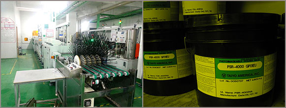
Most boards have a epoxy-ink soldermask printed onto each side to protect the copper surface and prevent solder shorting between components during assembly. Surface Coating, Image Transfer, Legend Printing, Final Curing. .
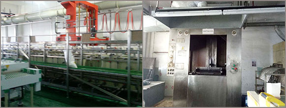
The copper component pads and holes have been left clear of soldermask. Now we apply a solderable surface finish to protect the copper until the components are soldered onto the board.There are a number of processing options that can occur depending upon the desired final finish. Currently at PCBAStore we can provide our customers with a SnPb or lead free solder finish, hard gold, Electroless Nickel Immersion Gold (ENIG), immersion tin or immersion silver. Other finishes include Organic Solderable Preservative (OSP), soft or bondable gold and a number of other “exotic”finishes like palladium..
Most PCBs have a component legend to show which component goes where. Ink is silkscreened onto one or both sides of the panel depending on the requirements of the customer. Today we use ink-jet printers to image the legends direct from the board digital data. Panels are then baked to cure the ink.
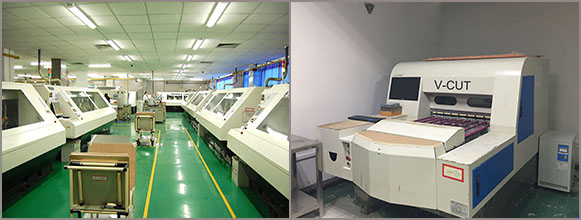
The next stage is to profile the PCBs and cut them out of the production panel to single pieces or arrays of varying sizes. Alternatively we can profile the individual circuits on a V-cut or CNC machine.
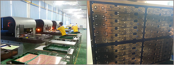
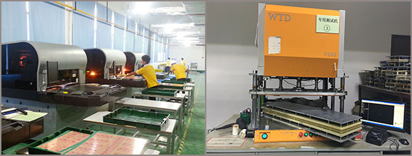
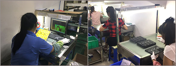
We electrically test every PCB whether multilayer or double layer against the original Gerber data. Using a flying probe tester or test jig we check each net to ensure that it is complete (no open circuits) and does not short to any other net. Shorts are repaired when possible and retested for verification.
In the last step of the manufacturing process a team of sharp-eyed inspectors give each PCB a final careful check-over to assure them meet requirements of our customers, industry specifications (IPC-A-600) and PCBAStore's standards, as well as having the physical dimensions and hole Sizes verified.
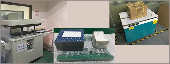
Printed Circuit boards meeting the acceptability standards are counted, shrink wrapped and readied for shipment along with all the required certificates, samples, cross sections, etc. They are individually packaged in protective plastic bags for storage or shipping with any methods which depends on the customer's requirements.
 Follow Us:


Contact Us: Please send Gerbers to svc@pcbastore.com for quotation
© pcbastore.com,All Rights
