General, quoting & support.
Add: Building E, No.58, Nanchang Road, Xixiang , Baoan District Shenzhen City, Guangdong, China
Tel : 0755-27348887
Fax : 0755-27349876
E-mail : svc@pcbastore.com
Blind Vias and Buried Vias
Simon / 2021-01-01
Contents [hide]
What Is A Blind Vias?

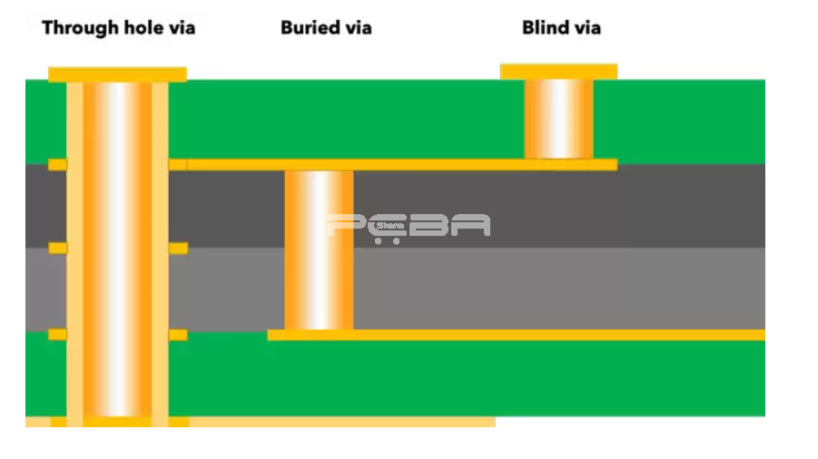
Blind vias are vias that connect an outer layer to at least one inner layer. In a PCB, there is always one outer layer either on top or at the bottom of the PCB, but there can be multiple inner layers. Because it only goes from an outer layer to an inner layer or layers, it does not ever pierce through the entire PCB and therefore is only visible on one side of the board. Sometimes when you are creating your PCB, you will find that one side will get full or packed before the other side, so you will no longer be able to drill the whole way through safely, so you will need to start using blind vias. The ability to add blind vias will significantly increase how much space you have available to you to use on your PCB.
There are four main kinds of blind vias that are mainly differentiated by how the blind via is created:
Photo defined blind vias
Sequential lamination blind vias
Controlled depth blind vias
Laser drilled blind vias
How Are The PCBs With Blind Vias Made?
As mentioned above, there are four main ways that blind vias are made, each with their own advantages and disadvantages depending on your specific situation.
Photo Defined Blind Via
To create a photo defined blind via, you need to start by laminating a sheet of photosensitive resin to a core and then covering that material with a pattern that covers where the holes are to be created. Once you expose the material to the correct wavelength of light, the material left exposed will harden, allowing you to immerse the PCB in an etching solution that will create the path for the holes for you. To finish the process, you will add copper plating to the hole and on the outer surface.
The main benefit of this method is that it costs the same to make hundreds as it does to create just one. But if you only need to make a few blind vias, it is not worth it.
Sequential Lamination Blind Via
To create the sequential lamination blind via you start by processing a thin piece of laminate in the same way you would create a two-sided PCB meaning the laminate will be drilled, then plated, then etched. The other side is a copper sheet (the first layer), and it is all laminated to the other layers of the board. This method is expensive, so should only be used as a last resort.
Controlled-Depth Blind Via
The controlled-depth blind via method is very similar to the method you would use to create a via the whole way through the PCB; only you will not go the whole way through. This is by far the least expensive method because you do not need to get any additional equipment, but you will need enough space on the board for the mechanical drill sized hole.
Laser Drilled Via
This type of blind via is made after the PCB is laminated but before the outer layer undergoes etching and lamination. There are different types of lasers that people use for this form of blind via creation, the most popular being the CO2 laser as it is one of the most powerful.
What Is A Buried Vias?
A buried via is used to create connections between inner layers, but it is not connected to any of the outer layers, and therefore cannot be seen from the outside. They are buried inside the PCB. A buried via can be made through any number of layers, though the layer count should be even (2, 4, 6, 8, 10, etc.) Keep in mind that buried vias are electroplated holes and need a separate drill file and therefore can be more expensive to create, but they do save you a lot of space on the outer layers and other layers that may not necessarily need to be a part of your buried via.
How Are The PCBs With Buried Vias Made?
When you create a buried via you start by making the inner layers that the buried vias will go through first. You will use your drill file to make the paths and then add your electro plating. Once you have your innermost layers made (or the ones with the buried vias) you can move on to building up until you eventually add the outside layers. Remember to test the vias before you add the outerlayers. That is one of the big differences between this type of via and others. You have to make them as you build the PCB, rather building the entire board (including the outerlayers) and then creating the vias or holes.
Advantages of Blind Vias and Buried Vias
The main benefit for both blind vias and buried vias is that you can add more connections, density, lines, and pads into your PCB design without actually adding to the overall layer count or having to increase the size of your board to make more space. Burried vias save space on both the outerlayers as it does not need to be connected to either outer layer. On the other hand, blind layers save space on one of the outerlayers as it does not go the whole way through, and it can also save space on some inner layers depending on how many layers you put the blind via through. Though, it is important to remember that if you do not go deep enough with your blind vias you can run into problems.
Disadvantages of Blind Vias and Buried Vias
The main disadvantage to both blind and buried vias is the cost. When you add buried and blind vias you are making the board more complex and therefore adding more manufacturing steps and more testing and precision checks. Now, there are different options when it comes to cost, especially with the blind vias as explained above, but you can expect that they will cost more than your typical vias that go the whole way through the board. However, for some people, the space and size savings are very much worth it or even necessary depending on the project.
They also tend to be more complicated or difficult to create than your typical hole-thru vias, so if you are new to creating PCBs, you may want to hold off on creating your own blind and buried vias until you have a little more experience with more basic vias.
Using Blind and Buried Vias in Altium Designer
Before you start working with blind and buried vias in Altium Designer, make sure that you have an understanding of how to work with regular thru-hole vias in Altrium Designer.
When you are making blind and buried vias on Altium Designer you will need to control where they start and stop, which you can do with the drill pair manager. When you add your pairs, you are telling Altium Deisgner which vias are in use and what their specific layers are. You can add multiple blind and buried vias, but it is important that you clearly label them so you will know which one is which in case you have to make adjustments.
Now you will move on to classifying and routing. You will classify your buried nad blind vias based on their routing density and purpose through rule priorities. When routing, you will represent your vias with the star key at the start and then click through each layer. Another option is using the Ctrl_Shift_Roll mouse wheel to go up or down through the individual layers. If your buried or blind via is spanning layers that you do not want it to, you can change the via drill pair in the property pannel.
After you place your vias, you will be able to edit them and move them the same way you can any other via, by dragging it around with your mouse.
Conclusion for Blind Vias and Buried Vias
In conclusion, blind and buried vias are both great options if you are looking to add more density, connections, lines, or pads to your PCB than the size seems to allow for. They both have similar advantages (adding more space) and disadvantages (more complex and therefore take more time and money to create), so which you end up using depends a lot on what your specific needs are. Blind vias connect one of the outer layers to one of more of the inner layers and a buried via connects two or more inner layers and cannot be seen on the outside of the PCB board.
You can use both blind and buried vias when designing a board through Altium Designer, though it is important to have an understanding of how to create and edit hole-thru vias before you get started as you will use many of the same tools and procedures. Once you have an understanding of hole-thru vias, it is fairly easy to start creating and editing both blind vias and buried vias.


