General, quoting & support.
Add: Building E, No.58, Nanchang Road, Xixiang , Baoan District Shenzhen City, Guangdong, China
Tel : 0755-27348887
Fax : 0755-27349876
E-mail : svc@pcbastore.com
All About PCB Hole Types: From Through-Hole to Microvias
PCBA Store / 2025-10-30
Contents [hide]
Printed Circuit Boards (PCBs) are the basic building blocks of almost every modern electronic gadget. They help link components both physically and electrically. A key part of designing a PCB is deciding where and how to place holes. These holes do many jobs, like holding parts in place, linking layers together, and keeping the board steady. Knowing the different kinds of holes on PCBs is super important for creating and building effective designs.

An In-Depth Look at PCB Hole Varieties
Getting to know the various holes on PCBs is a must for engineers and designers who want to boost performance, dependability, and ease of production.
Through-Hole
Through-Hole: These are the most usual holes you’ll see on PCBs. They go all the way from the top of the board to the bottom. Often used in older or super sturdy designs, through-holes are great for strong physical connections. They work well with leaded parts that get soldered on both sides.
Plated Through Holes (PTH)
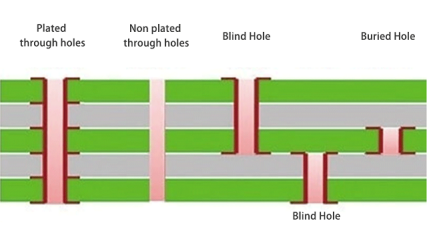
Plated Through Holes (PTH): These holes have a special conductive layer inside. This helps join traces across different layers of the PCB. PTHs are vital for mounting parts and making vias that keep electrical flow between layers.
Non-Plated Through-Holes (NPTH)
Non-Plated Through-Holes (NPTH): Unlike PTHs, these holes don’t have a conductive layer. They’re used for mechanical tasks, like fastening the PCB with screws or lining things up during setup. NPTHs don’t help with electrical links but are key for keeping the board strong.

Buried Via
Buried Via: This kind of hole links two or more inner layers of a PCB but doesn’t reach the outer sides. Buried vias help pack more routing into tight spaces. They’re often found in High-Density Interconnect (HDI) boards where room is scarce.
Blind Via
Blind Via: This hole ties an outer layer of the PCB to one or more inner layers. But it doesn’t cut through the whole board. Blind vias save space on the surface and allow for trickier multilayer setups, especially in small gadgets.
Countersink and Counterbore Holes
These unique mechanical features are made to fit certain fasteners. They keep the board flat and working well without any issues.
Counterbore Holes
Counterbore Holes: These are regular screw holes with a cylindrical shape. They’re drilled into the board’s surface to snugly hold a typical socket cap screw with a slightly curved head. Their size—both width and depth—is figured out carefully based on the screw’s details.
Countersink Holes
Countersink Holes: Unlike counterbore holes, these are cone-shaped. Drilling this kind of hole takes extra care and planning compared to a counterbore. They let flathead screws sit even with or below the surface, keeping everything smooth across mounting areas.
Tool Hole
Tool Hole: This hole is used to attach the circuit board to a test setup or its working spot. These non-plated holes help with alignment during automated testing or assembly steps.
Microvia
Microvia: These are tiny vias, usually with a width of less than 0.15 mm. They’re a must in HDI boards where small size and clear signal flow matter a lot.
Sidestep Hole
Sidestep Hole: These holes are drilled before through-holes. They’re often used to secure or weld specific parts. Their special placement makes them handy for unique tasks that need early alignment or extra support for components.
Crimp Holes
Crimp Holes: These are half-drilled holes meant for connecting wires to the PCB during hand soldering. Crimping offers a solid spot for wire leads without weakening the board’s structure.
Slot Holes
Slot Holes: These are for parts with odd-shaped leads or to add specific mechanical details in the PCB layout. Slot holes can be plated or non-plated, depending on their job. This gives flexibility for both electrical and physical designs.
Importance of Proper Hole Design
The smart placement and careful design of different holes on PCBs play a big role in how efficiently they’re made, how reliable they are, how well they handle heat, and how much they cost. Good hole design means the PCB can be built dependably and without breaking the bank. Bad design, though, can cause mistakes during production and drive up costs.
How well a PCB works electrically often depends on using vias the right way. Plated through-holes, blind vias, buried vias, and microvias make sure electrical connections between layers are solid. Meanwhile, non-plated through-holes, countersinks, counterbores, and slots give physical strength and help secure the PCB in its case.
Also, heat can be managed better with certain via setups, like thermal vias in plated through-holes. Proper hole design helps with cooling by letting heat escape more easily.
Knowing these differences helps engineers not just meet the needed functions but also smooth out assembly steps and lower the chance of problems down the road.
get instant online quote from PCBA Store : PCB Prototype & PCB Fabrication Manufacturer
If you’re looking for trusty fabrication services that handle all kinds of PCB hole setups—from basic through-holes to tiny microvias—PCBA Store has you covered with over 16 years of know-how. Based in China, they’re a top PCB manufacturing and assembly company. They’ve been providing full electronic manufacturing solutions for 16 years.
Their skills cover everything from early prototypes to large-scale production. They serve many fields like medical tools, car systems, factory automation, communication gear, everyday electronics, robotics, and more. From PCB design and layout to prototyping, mass production, and assembly, their Printed Circuit Boards are widely used in robotics, medical, and automotive industries.
You can quickly get a custom online quote for your project using their easy quoting tool. Their online quotes are over 95% accurate. They also offer Turnkey BOM Sourcing, and 10PCS Assembly starts at just $100. Whether you need Flex PCBs with microvias or rigid boards with buried or blind vias, PCBA Store delivers top-notch results fast.
Their modern facilities can manage all types of via tech, including laser-drilled microvias.


