General, quoting & support.
Add: Building E, No.58, Nanchang Road, Xixiang , Baoan District Shenzhen City, Guangdong, China
Tel : 0755-27348887
Fax : 0755-27349876
E-mail : svc@pcbastore.com
How Rapid Prototyping PCB is Revolutionizing PCB Manufacturing in Terms of Growth
PCBA Store / 2025-10-29
Contents [hide]
Introduction to Rapid Prototyping PCB
Rapid prototyping PCB is changing the electronics world. It helps companies keep up with the need for quick, small, and strong devices. The global rapid prototyping PCB assembly market was worth $4 billion in 2023. Experts say it will grow to $6 billion by 2028, with a 9.1% yearly increase. This method is shaking up how PCBs are planned, checked, and made in big numbers. It uses smart machines, digital tools, and super-accurate building methods. These cut the time to make prototypes from weeks to just days. This pushes growth in fields like IoT, cars, and medical tools.

Overview of Rapid Prototyping PCB
Rapid prototyping PCB speeds up making printed circuit boards. It mixes digital design tools like CAD/CAM with new building tricks. This creates working prototypes in just 24-48 hours. Unlike old ways with slow etching and plating, this method makes work faster and more exact. Here are the main parts:
· Digital Design and Testing: Tools like Altium Designer make Gerber files. Special tests, like finite element analysis (FEA), check electrical, heat, and strength issues. This cuts design mistakes by up to 30%, according to iNEMI reports.
· Material Choices: It works with 1-64 layers using FR-4, Rogers RO4350B for RF, or polyimide for bendy PCBs. This fits many uses.
· High-Tech Building: Laser direct imaging (LDI) makes tiny 2.5/2.5 mil lines and spaces. CNC milling and inkjet printing handle complex HDI designs.
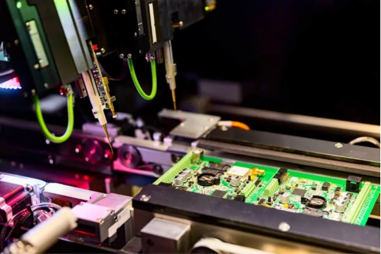
· Fast Assembly: SMT machines place over 100,000 parts per hour. AOI and X-ray checks ensure 99.5% perfect boards.
From hand-soldered boards in the 1940s to photolithography in the 1980s, rapid prototyping PCB now uses cloud tools and 3D printing. This makes it easy for everyone to use. Teams worldwide can work together in real-time and tweak designs fast. For big fields like aerospace, it meets IPC-A-610 Class 3 rules. Startups love it for small runs (1-100 units) with no minimum order. This checks designs for signals up to 100 GHz for RF and sparks new ideas in small devices. It sets companies up to win in a tough market.
Benefits of Rapid Prototyping PCBs
Rapid prototyping PCB changes how efficient, cheap, and creative manufacturing can be. It gives companies a big advantage. Here’s a closer look:
Accelerated Development and Market Entry
With 5G and AI devices needing to launch in 6-9 months, rapid prototyping PCB shortens design-to-prototype time by 70-80%. Fast services deliver 2-layer boards in 24 hours. Four-layer boards take 3-5 days. This lets companies test with users early and get market feedback quicker.
Cost-Effective Iterations
Old PCB changes cost $5,000-$10,000 each time because of setup fees. Rapid prototyping skips those costs. Ten 2-layer boards start at just $5. Spotting flaws early with digital tests saves 40% on project money, says a 2024 Deloitte study.
Enhanced Design Precision
Super-accurate LDI and tiny microvias (down to 4 mil) make reliable HDI designs for wearables. AOI and X-ray checks meet IPC Class 2-3 standards. This cuts field failures by 25%.
Innovation and Flexibility
Engineers can try aluminum for LED cooling or PTFE for RF uses without spending much. This leads to 20% more design options, per McKinsey’s 2025 report. It helps create foldable gadgets.
Early Validation and Compliance
In-circuit testing (ICT) and functional testing (FCT) catch problems like overheating. This cuts recalls by 50%. Following RoHS, UL, and REACH rules ensures products are ready for sale.
Scalable Production
Moving from prototypes to million-unit runs is easy. Turnkey assembly finds parts worldwide. This works for small markets or big orders without losing quality.
These perks lead to 15-20% faster money-making cycles, says Gartner. This fuels growth for companies.

Key Technologies Driving Rapid Prototyping PCB
The rapid prototyping PCB market is set to hit $9.65 billion by 2030, growing at 20.07% yearly. New tech makes it more exact, fast, and able to grow. Here are the top advancements:
Laser Direct Imaging (LDI) for Ultra-Fine Traces
LDI uses UV lasers instead of old photolithography. It etches lines as thin as 2 mil with ±0.1 mil accuracy. This makes HDI boards with 0.4mm pitches, key for 5G and IoT gadgets. It cuts building time by 50% compared to mask methods.
Additive Manufacturing (3D Printing)
Inkjet and aerosol jet printing use conductive inks, like silver nanoparticles, to make multi-layer PCBs in hours. This cuts waste by 90%. It’s used in 25% of car EV prototyping, says a 2025 IDTechEx report. It handles tricky shapes like built-in parts.
Automated Optical Inspection (AOI) and X-Ray Systems
AOI scans at 100 cm²/s, spotting issues like solder bridges with 99.9% accuracy. X-ray systems find hidden flaws in BGAs, ensuring reliability for aerospace (IPC Class 3). These boost first-pass success by 15%.
High-Speed SMT and Robotics
Smart robots and vision-guided SMT machines place tiny 0.3mm parts at 150,000 per hour. With AI, they handle mixed THT/SMT setups, boosting output by 40% while keeping super-accurate.
Cloud-Based Design and Simulation Platforms
Cloud tools like Autodesk Fusion 360 let teams edit together in real-time. They cut delays by 25%. Virtual tests predict signals for 100 GHz RF, reducing physical remakes.
Advanced Materials for Specialized Applications
High-frequency materials like Rogers RO4003C work for 5G with low signal loss (Dk < 3.5). Flexible polyimides allow bends down to 0.5mm for wearables. The rapid prototyping materials market will hit $4.7 billion by 2035 at 18.1% yearly growth.
IoT-Enabled Process Monitoring
IoT sensors watch machines and materials in real-time. They save 15% on energy and predict maintenance with 95% accuracy. This keeps quality steady for varied, small-batch runs.
These advancements make rapid prototyping PCB a $20.5 billion leader in electronic prototyping by 2033, with a 6.8% yearly growth. They help companies meet tough demands for accuracy, speed, and eco-friendliness in a super-competitive market.
FAQ
What is rapid prototyping PCB, and why is it critical for manufacturers?
Rapid prototyping PCB uses smart tools and digital steps to make working PCBs in 24-48 hours. It helps check designs fast and get products to market sooner. It’s key for staying ahead in fields like IoT and cars.
How cost-effective is rapid prototyping PCB for small runs?
Prices start at $5 for ten 2-layer boards. Turnkey assembly costs $80. It skips setup fees, saving up to 40% on budgets with early error checks.
What are typical lead times for rapid prototyping PCB?
Fast services give 2-layer boards in 24 hours. Multi-layer boards take 3-5 days. Full prototypes ship in 1-10 days, based on complexity.
Which sectors rely on rapid prototyping PCB?
Gadgets, cars (EV systems), medical tools, aerospace, and telecom (5G) use it for quick changes and reliable prototyping.
How do advanced technologies improve rapid prototyping PCB?
LDI, 3D printing, and AI tools boost accuracy, cut waste by 90%, and shorten timelines by 50%. They support complex HDI and bendy designs.
Partner with PCBA Store for Cutting-Edge Rapid Prototyping PCB Solutions
Electronics firms, OEMs, and design teams looking to speed up innovation in 2025 can trust PCBA Store. Based in Shenzhen’s electronics hub, PCBA Store has over 16 years of know-how. Our rapid prototyping PCB services offer 24-hour express prototypes (1-64 layers, HDI, rigid-flex) and turnkey assembly for up to 1 million units. Enjoy no minimum orders, instant online quotes, 99% on-time delivery via DHL, and ISO-certified quality with full refunds for defects. Upload your Gerber files at PCBA Store.com for a free DFM review and $50 coupon. Or contact svc@pcbastore.com (+86-755-27348887) to streamline your product creation with accuracy, speed, and growth tailored to your needs.


