General, quoting & support.
Add: Building E, No.58, Nanchang Road, Xixiang , Baoan District Shenzhen City, Guangdong, China
Tel : 0755-27348887
Fax : 0755-27349876
E-mail : svc@pcbastore.com

Heavy Copper PCB: Copper Thickness and Manufacturing
PCBA Store / 2026-11-19
Contents [hide]
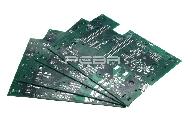
A heavy copper printed circuit board is a board whose conductor thickness is increased to carry current or spread heat through selected parts of its copper pattern.
Copper Weight and Finished Thickness
It is the weight of one square foot of copper foil.
Alternatively, heavy copper may be employed for heat dissipation from components including surface-mounted ones. In that case, the copper acts as a heat spreader to a larger area of the board, or to a metal substrate.
The term 'heavy copper' is not precise. It may mean a board in which the whole of one or both layers is made of thick copper foil, or a board in which the greater part of the copper is of relatively thin foil but certain areas (such as conductors) are increased in thickness by plating. In many cases, such as the 'copper coin', the thick copper is inserted into a cut-out in the board and is not plated on to it.
RFQ detail | Purpose |
Copper by layer | Where added copper goes |
Current and temperature rise | Electrical and thermal target |
Finished trace width and spacing | Etch allowance review |
Hole plating | Layer-to-layer current path |
Current Paths and Heat Flow
The term 'hole wrap' may be used to describe the plating of copper over the edge of the hole, connecting the wall plating to the surface foil. In drilling a hole in heavy copper, care must be taken to see that the hole is not obscured, that the plating is continuous over the hole wrap, and that the drill does not produce a 'smear' of copper which would lead to a short circuit or to an unreliable connection.
Etching and Trace Geometry
Thick copper takes longer to etch and the surface of the copper will be exposed to the etchant for a long time. The etchant used should be selected to minimise undercutting. The resist applied must be strong enough to withstand a long etch and it may be necessary to use a resist which can be applied in a thick layer.
It is necessary to allow increased spacing between conductors (to allow for side etching) and rounding of sharp corners in the artwork.

Drilling and Plated Connections
Heavy copper foil has to be drilled with care; the drill may be deflected by the copper or the copper may be smeared across the hole. Entry and exit material has to be chosen to minimise these effects.
In heavy copper boards, holes are often required to carry a high current, and a close watch must be kept on the thickness of the plated copper deposited in the holes to make sure the specified minimum thickness is reached.
Applications in Power and Control Boards
Heavy copper may be needed to carry current (in circuits such as power supplies, converters or motor control equipment) or to spread heat (for instance in surface-mount technology boards). PCBA Store's heavy copper PCB manufacturing services page gives the relevant process details.
Current and Thermal Use
This demand grew from the power supply industry and from manufacturers of communications equipment. Voltage drop and heat generation are the main concerns of the power supply designer. PCBA Store's thick copper PCB capability page gives the relevant process details.
The use of heavy copper in circuit boards has long been associated with higher current paths, and the ability of the finished board to carry current has usually been calculated by considering the copper pattern area. PCBA Store's copper thermal management designs page gives the relevant process details.
The designer should remember that current-carrying capability is sometimes limited not by the copper conductors but by such features as the current-carrying capability of the connectors or by the solder joints.
A thick copper PCB can suit a high-current path, while heavy copper for thermal management must still account for the components, vias, joints and connectors that complete the heat path.
Details for a Heavy Copper PCB RFQ
It is preferable to keep the current-carrying path within one layer (e.g., the outer layer) rather than transferring from an outer layer to an inner layer, or from one side of the board to the other, since the current-carrying capability of the hole is restricted. It is better to have a number of small holes in parallel than a single large hole, but this is not always practicable.
Current Route and Plated Holes
The plating of a large hole is difficult because the throwing power of the plating solution is limited, and it may be necessary to specify a minimum plating thickness and to check it in each batch.
When heavy copper is used in contact areas (e.g., in a connector) care has to be taken to avoid the tarnishing of the copper, which may cause high contact resistance. If possible, such areas should be protected by gold plating, or by a suitable organic coating.
PCBA Store Heavy Copper and HDI Capabilities
PCBA Store supports heavy copper construction up to 6 oz for mass production and 30 oz for samples, and offers partial heavy copper among its rigid PCB processes.
Practical Takeaway
Start with the current path and its heat load, then list copper by layer so the fabricator can see where thickness changes.
For project-specific scope and timing, contact PCBA Store.
FAQ
What Does Heavy Copper Mean?
It can mean thick foil across a layer, selective plating on traces, or a local insert such as a copper coin. Specify the intended construction.
Does Thicker Copper Solve Every Heating Problem?
No. A via, solder joint, connector or enclosure interface may limit the full heat path even when the conductor is thicker.
Why Can Heavy Copper Change Trace Geometry?
Longer etching can undercut the resist, so review finished trace width and spacing rather than relying on artwork dimensions alone.
What Details Belong in a Heavy Copper RFQ?
List copper weight by layer, current duty, temperature-rise limit, finished trace sizes and any minimum hole-plating thickness.
What Capacity Does PCBA Store Offer?
Check the published limits against the proposed stackup, order quantity and need for partial heavy copper before releasing the drawing.
Previous article:Fast-Turn PCB Prototypes: What Sets the Lead Time?



