General, quoting & support.
Add: Building E, No.58, Nanchang Road, Xixiang , Baoan District Shenzhen City, Guangdong, China
Tel : 0755-27348887
Fax : 0755-27349876
E-mail : svc@pcbastore.com

Via-in-Pad and HDI Microvias for Fine-Pitch PCBs
PCBA Store / 2026-11-20
Contents [hide]
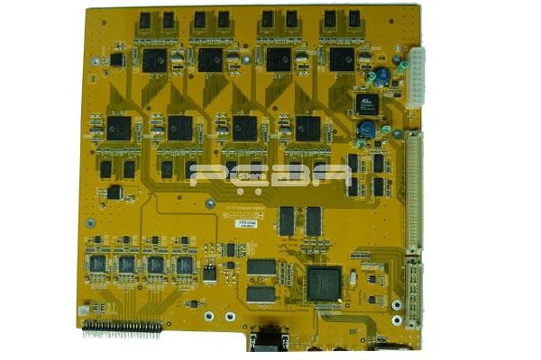
A via-in-pad connection is a plated hole placed within a component pad, while high-density interconnection uses smaller features and selected layer transitions to make routing space in a compact board.
Via-in-Pad in Fine-Pitch Layouts
The key consideration in connecting to a component pad is the reliability of the joint, whether it is a soldered joint for a through-hole device or a surface mount, or a wire bond pad. There is also a process consideration: solder paste is printed onto a pad and the paste may be drawn into a via by capillary action. The shrinkage of the solder paste during reflow, plus the solder drawn into a via-in-pad, can create an unsatisfactorily small fillet, leading to an unreliable joint. This is particularly true with a pad that has a via within it. If the via is not tented or plugged, solder will be drawn into it.
A via in pad arrangement may shorten an escape path, but the pad finish and solder process need to suit the selected package.
Structure | Connection |
Through-via | Outer layer through the complete stack. |
Blind via | Outer layer to a selected inner layer. |
Buried via | One inner layer to another inner layer. |
Microvia | A small, usually laser-drilled layer transition. |
Tented Vias and Openings
Tenting consists of applying the solder mask over the via hole and its annular ring so that material bridges over the hole. Unfortunately, when the varnish dries, stresses set up and the mask may crack with the result that a small hole appears at the top of the via. Then, when components are reflowed, solder is drawn through the crack.
If tenting cannot be successfully carried out because of hole size or track density, then the vias can be plugged with a suitable paste. The stencil should be positioned so that the paste is only deposited onto the vias to be plugged.
Laser-Drilled Microvias
The increase in demand for HDI multilayer boards has led to the use of laser-drilled microvias of less than 0.1 mm diameter, which are smaller than conventional plated through-holes. The quality of the via is important, in order to avoid a poor plating job. PCBA Store's via-in-pad PCB fabrication page gives the relevant process details.
The microvia is typically formed by laser, and connects two adjacent layers. The shape of the holes is important, both for reliable plating and for filling. The annular ring must be sized so that the laser beam can hit the target area accurately, and so that a reliable plated connection is made to the lower copper layer. PCBA Store's HDI microvia board capability page gives the relevant process details.
Blind and Buried Vias
Layer Transitions
The commonest forms of interconnection are: plated through-hole (from the outside through all the layers), blind via (from an outside layer to an inner layer) and buried via (from one inner layer to another inner layer). Microvias, however, are typically produced by laser drilling, which forms smaller holes. They are formed sequentially: a sub-assembly is made, microvias are drilled and plated, then further sub-assemblies are added.
One limitation is that a microvia is usually used only for connections between adjacent layers.
Stackup and Sequential Lamination
In the construction known as sequential build-up (SBU), the package has a core, to which are added alternate layers of conductor and dielectric, each layer being drilled and plated as it is added. In this way the layer count is built up one layer at a time.
A stacked via is one in which a via hole appears in the same location on successive layers, so that the hole stack goes through more than one layer. In a staggered via, the vias are offset from one another, so that the connection is made through the copper pads rather than directly through the vertical stack.
Assembly Checks for Fine-Pitch Boards
The assembly of fine-pitch components relies on accurate positioning of the component and the printed circuit board, and on careful control of the reflow process. The land pattern design must be matched to the component and the process. PCBA Store's blind and buried via PCB manufacture page gives the relevant process details.
The assembly process for fine-pitch components has become more demanding with the increase in the use of area array packages (ball grid arrays and chip-scale packages).
The track width and spacing must be compatible with the manufacturing capability, and the resulting impedance must be acceptable.
The pad length should be sufficient to allow a good solder fillet to be formed.
Details to Confirm Before Ordering HDI PCB
The base material selection, copper foil thickness, prepreg and solder mask are crucial to the manufacture of a fine pitch board.
However, the thinner the copper, the more care is needed in handling; and the risk of damage increases.
Solder mask thickness and resolution are important.
The surface finish must be compatible with fine pitch assembly.
The fabrication process should be designed for the specific board, and the design should take into account the process capability.
The reduction in the size of the plated through-hole is limited by the aspect ratio (board thickness divided by hole diameter).
Reducing the diameter of the hole to allow an increase in density must be matched by an improvement in the plating process, to ensure that the plating thickness at the centre of the hole is sufficient.
PCBA Store Via-in-Pad and HDI Capabilities
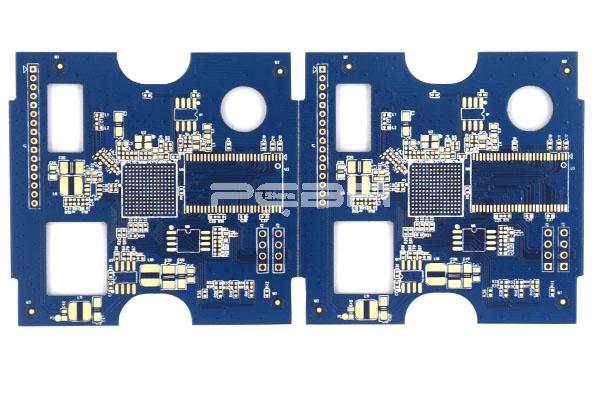
PCBA Store supports via-in-pad, buried and blind holes, and laser-drilled microvia boards. Its listed laser drill sizes are 0.1 mm for mass production and 0.075 mm for samples.
The capabilities of the manufacturer must be matched to the design. The tracks, spaces and holes of a fine pitch board can be at the limit of the capabilities of a manufacturer, so it is essential to check that the manufacturer's process capability is adequate.
The board designer should also be aware of the effect of design on yield.
The tighter the design rules, the higher the probability of a defect and the lower the yield.
The cost of a board with fine-pitch features is therefore significantly higher than that of a similar design with less demanding features.
The manufacturer's capability data should be used to determine the design rules.
An HDI PCB combines smaller interconnect features with selected layer transitions; specify the stackup and drill construction needed for the layout.
Practical Takeaway
Use advanced interconnect where the component field or routing density needs it. Confirm layer transitions, hole geometry, fill and assembly consequences before release.
PCBA Store supports PCB fabrication and assembly; confirm the selected interconnect structure against the released stackup and assembly plan.
For project-specific scope and timing, contact PCBA Store.
FAQ
Does Every BGA Need Via-in-Pad?
No. The package pitch, pad geometry and available routing layers determine whether it is needed.
What Is a Tented Via?
It is a via opening covered by solder mask; it does not create the same filled and planar surface as via-in-pad.
Why Are Microvias Used in HDI Boards?
Their smaller transitions can free routing space in dense layouts, subject to the fabricator’s process limits.
What Is the Difference between Blind and Buried Vias?
A blind via connects an outer layer to an inner layer; a buried via connects inner layers only.
What Laser Drill Sizes Does PCBA Store Offer?
PCBA Store uses 0.1 mm for mass production and 0.075 mm for samples; confirm the required stack and availability.



