General, quoting & support.
Add: Building E, No.58, Nanchang Road, Xixiang , Baoan District Shenzhen City, Guangdong, China
Tel : 0755-27348887
Fax : 0755-27349876
E-mail : svc@pcbastore.com

How to Reduce PCB Manufacturing Costs Without Compromising Quality
PCBA Store / 2026-08-27
Contents [hide]
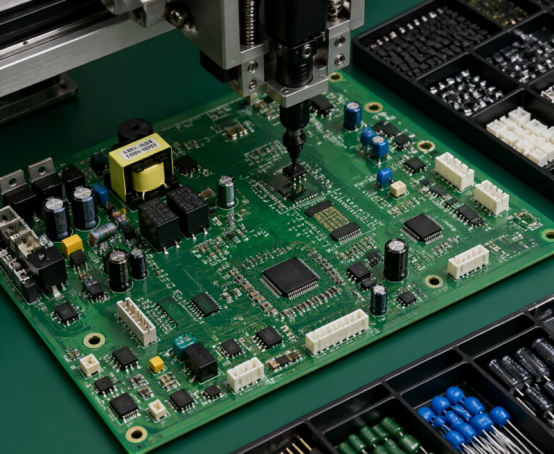
PCB manufacturing cost is controlled long before fabrication begins. Layer count, panel utilization, materials, feature sizes, component selection, testing, and order planning all affect the final price. The practical goal is not to remove necessary controls, but to eliminate specifications and production steps that add cost without improving product performance.
Understand What a PCB Quote Actually Includes
A PCB quote reflects the resources required to manufacture a bare board. The main variables include board dimensions, quantity, layer count, material, thickness, copper weight, trace and spacing limits, hole size, surface finish, via treatment, controlled impedance, and special structures such as blind vias.
PCB assembly is calculated separately because it involves another set of operations. Component sourcing, stencil preparation, SMT placement, THT insertion, reflow, manual soldering, inspection, programming, functional testing, coating, depanelization, and box build can all affect the total PCBA price.
A PCB cost estimator is therefore useful for initial comparison, but it does not represent the complete cost of an assembled product unless every required service is included. At PCBA Store, our online system separates PCB fabrication parameters from assembly inputs such as BOM lines, SMT and THT quantities, BGA or QFN devices, assembly sides, testing, and additional processing.
Cost area | Main pricing inputs | Typical cost risk |
Bare PCB | Size, layers, material, copper and finish | Unnecessary technical specifications |
Components | BOM lines, availability and approved sources | Shortages or obsolete parts |
Assembly | Placement count, package type and board sides | Manual work and repeated process steps |
Testing | AOI, X-ray, ICT and functional testing | Inadequate test planning |
Delivery | Quantity, production time and shipping | Unplanned expedited service |
Apply DFM Before Finalizing the PCB Design
Design for Manufacturing, or DFM, connects electrical design decisions with factory capabilities. A design outside the manufacturer’s standard process window may require extra engineering review, specialized equipment, tighter process control, or a lower expected yield. Each condition can raise PCB cost.
Layer count deserves an early review. Every added layer requires more material, imaging, alignment, lamination, and inspection. Reducing a six-layer board to four layers may save money, but it is only appropriate if the revised stack-up still supports routing density, impedance, return paths, power distribution, thermal control, and EMC performance.
Feature sizes follow the same principle. Very narrow traces, tight spacing, small drilled holes, high via aspect ratios, blind vias, and buried vias may be essential in a compact high-density design. They should not, however, become default requirements. PCBA Store’s online PCB quote options illustrate the pricing distinction between trace and spacing below 4/4 mil and standard rules of 6/6 mil or above. The system also separates 0.1 mm vias from holes of 0.3 mm or larger.
Good DFM does not force every board into the simplest construction. It identifies where advanced technology creates real product value and where it only creates manufacturing difficulty.
Improve Board Size and Panel Utilization
Board dimensions influence more than material consumption. They determine how many circuits fit on a production panel and how much laminate becomes unusable around tooling borders, routing paths, and process coupons.
A small dimensional adjustment can sometimes improve panel utilization without changing circuit performance. That decision must consider mounting holes, enclosure clearances, connectors, creepage distances, and mechanical strength. Cutting the outline merely to reduce area may create a more expensive assembly or enclosure problem later.
Panel design also affects PCBA production. Rails, fiducials, tooling holes, component-to-edge clearance, V-scoring, and routed tabs must support printing, placement, reflow, inspection, and separation. We recommend confirming panelization with the manufacturer before releasing the production files, especially when different designs share one panel or X-out acceptance is restricted.
Match Materials and Finishes to the Application
Material selection should be based on operating conditions rather than a general preference for a higher grade. Standard FR-4 can support many commercial applications, while higher-Tg FR-4, aluminum, Rogers, ceramic, or PTFE materials serve more specific thermal or high-frequency requirements.
Copper weight also needs engineering justification. Heavier copper can support higher current and improve thermal performance, but it uses more material and may require wider manufacturing allowances. Selecting 2 oz or 3 oz copper for every design increases PCB manufacturing cost without providing a benefit when 1 oz copper already meets the electrical and thermal requirements.
Surface finish should follow assembly and end-use needs. Lead-free HASL may suit many standard boards, while OSP, immersion gold, immersion silver, or immersion tin may be selected for flatness, fine-pitch assembly, shelf-life, contact, or process requirements. The lowest-priced finish is not economical if it causes solderability problems or shortens usable storage life.
Control PCB Assembly Cost Through the BOM
Components often account for a large share of the complete PCBA budget. A reliable PCB assembly cost calculator therefore needs a complete BOM with manufacturer part numbers, quantities, reference designators, package details, and approved alternatives.
Too many unique parts increase purchasing and material-management work. Designers can reduce this burden by standardizing resistor and capacitor package sizes, consolidating equivalent values where the circuit permits, and avoiding uncommon components without a clear technical need.
Availability matters as much as unit price. A low-cost component with a long lead time, high minimum order, or uncertain lifecycle can delay the full build. Approved equivalent parts give procurement teams room to respond to supply changes, but substitutions must be reviewed for footprint, rating, tolerance, compliance, and functional compatibility.
PCBA Store supports turnkey, partial-turnkey, and consigned component models. The right option depends on purchasing control, existing inventory, traceability requirements, and the customer’s approved supplier policy.

Design the Board for Efficient Assembly
Assembly cost rises when a board requires more machine cycles or manual handling. Double-sided SMT needs another printing, placement, and reflow sequence. Mixed SMT and THT production introduces insertion and soldering operations after surface mounting. Fine-pitch ICs, BGA, QFN, and other leadless packages may also require more detailed process control and inspection.
Component layout can reduce avoidable work. Consistent orientation, adequate placement clearance, accessible test points, clear polarity marking, suitable fiducials, and practical panel support improve assembly flow. Complete manufacturing data also prevents delays. A PCBA package should normally include Gerber files, a BOM, centroid data, and assembly drawings with revision control.
Our assembly capabilities cover SMT, THT, mixed technology, and single- or double-sided placement. Published package capabilities include components down to 01005 and pitch specifications down to 0.4 mm, but using the smallest available package is not automatically the most economical decision.
Balance Quantity, Lead Time, and Inventory
Higher quantities spread setup and engineering charges across more boards, lowering the apparent unit price. That saving becomes false economy when unused boards remain in inventory after a design revision or demand change.
Prototype and pilot orders should confirm electrical operation, manufacturability, assembly yield, and test coverage before volume production. After validation, larger batches can improve material purchasing and production efficiency.
Lead time also changes the PCB quote. Expedited production may require priority scheduling and additional factory capacity. Standard lead time is normally more economical when the project schedule allows it. PCBA Store supports prototype, low-volume, and mass-production orders, allowing quantity to follow the project stage instead of an arbitrary minimum.
Keep the Quality Controls That Prevent Larger Losses
Inspection should be selected by production risk, not removed as a general cost-saving measure. Visual inspection can identify basic workmanship issues. AOI checks placement, polarity, missing components, and visible solder conditions. X-ray inspection examines hidden joints beneath BGA and QFN packages. ICT checks circuit connections, while functional testing confirms that the assembled board operates according to the customer’s procedure.
Board condition | Relevant control | Cost protected |
Dense SMT placement | AOI | Rework and placement defects |
BGA or QFN packages | X-ray | Hidden solder-joint failures |
High circuit complexity | ICT | Opens, shorts and value errors |
Product-specific operation | Functional testing | Field failures and returns |
Removing a necessary test may lower the initial PCBA price while increasing rework, returns, diagnosis time, and warranty exposure. Cost optimization should instead improve first-pass yield and apply the appropriate test at the correct production stage.
Compare Quotes on the Same Manufacturing Scope
A meaningful comparison requires identical technical and commercial inputs. Buyers should align board specifications, quantities, component sources, test coverage, delivery terms, tooling, shipping, and optional services before comparing totals.
Unit price alone can also mislead. A supplier offering a low unit cost with a high minimum quantity may create a larger total purchase than a supplier supporting the quantity actually required. The full project cost—including unused inventory and logistics—is the better purchasing measure.
For a more accurate budget, use the PCBA Store instant online quote to test different PCB and PCBA specifications. You can also upload Gerber files, BOM data, centroid files, and assembly drawings for engineering review. If a material or process is outside the online options, contact our support team for a manual quotation and DFM discussion.
FAQ
What has the greatest effect on PCB manufacturing cost?
Layer count, board area, material, copper weight, feature size, via structure, surface finish, quantity, and lead time are the main fabrication cost drivers. Their impact varies with factory capability.
Can PCB layer count be reduced safely?
Layer count can be reduced when the new stack-up still meets routing, impedance, return-path, power, thermal, and EMC requirements. Electrical validation must come before cost savings.
Why is the final PCBA price higher than the PCB quote?
A bare PCB quote excludes components and may also exclude stencil preparation, assembly, testing, programming, coating, box build, and shipping. These items must be included separately.
How accurate is a PCB cost estimator?
Accuracy depends on the input. Dimensions alone provide only a rough estimate. Complete stack-up, material, copper, finish, drill, quantity, assembly, BOM, and testing data produce a more useful result.
Does ordering more PCBs always reduce total cost?
A larger order usually lowers unit cost by spreading setup charges, but it can increase total spending and inventory risk. Production quantity should follow validated demand and the design stage.
Previous article:Global PCB Assembly Supply Chain Guide



