General, quoting & support.
Add: Building E, No.58, Nanchang Road, Xixiang , Baoan District Shenzhen City, Guangdong, China
Tel : 0755-27348887
Fax : 0755-27349876
E-mail : svc@pcbastore.com
What is Silkscreen on PCB?
Simon / 2021-02-05
Contents [hide]
A simple analogy from which to observe a silkscreen would be observing a map, especially a countered map. We know that the various features are labeled on the map; otherwise, it would make no sense to see the lines without a label. For a feature to be easily identifiable, there must be an accompanying name or standard symbol to denote it.

What is PCB silkscreen?
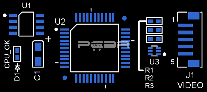
When it comes to Printed Circuit Boards (PCBs), the silkscreen is the ink layer that provides printed information to identify the various circuit points, components, marks, logos, warning symbols, etc. The silkscreen is mostly applied on the components side since it's economically more viable than if applied on the solder side. There are some PCBs you'll find with a silkscreen on the solder side.
The silkscreen employs a highly formulated epoxy ink. It is also necessary that the ink be non-conductive. For these reasons, the ink is usually available in a few colors, i.e., white, black, yellow.
When applied as per standards, a detailed silkscreen makes the work easier for both the engineer and the manufacturer. All components can be identified easily, and circuits efficiently traced.
What information does PCB silkscreen provide?
You can already guess what information the silkscreen provides. The silkscreen is, however, not a functional part of a PCB. The information displayed include:
Warning symbols
Reference designators for identifying the part's location
Test points designators
Board identification numbers
The polarity of the different parts
Logos and manufacturer or version numbers
Methods of PCB silkscreen printing
There are basically three common methods of PCB silkscreen printing. These methods differ in aspects such as overall cost, time to complete the printing, the available board spacing, and the printed circuit board material to be used. Each method has its uniqueness, which determines where that particular method can be applied.
The common PCB silkscreen printing methods are:
Manual Screen Printing
Liquid Photo Imaging (LPI)
Direct Legend Printing (DLP)
1. Manual Screen Printing
This is the oldest of the three methods and happens to be the least expensive. However, this method is limited to line widths not less than 0.007", or when the registration tolerance is at 0.005". A stencil made of text and traces is used to direct the epoxy ink through. The traces are usually nylon-made. Next, the laminate is placed in the baking oven to cure the ink.
The main advantages of manual screen printing are the ease and low costs associated with this method.
There are significant limitations, however. First, the method requires bigger board spacing to accommodate the large text size.
Pad clearance is also bound to be troublesome in manual screen printing.
Lastly, it takes long, typically years, to master the art of manual screen printing. It's surely not for the faint-hearted.
2. Liquid photo imaging (LPI)
If the minimum line width required is 4mil, LPI can be applied. If you're conversant with solder mask application, you may already know how LPI is done.
Generally, the laminate is coated with an epoxy layer. The epoxy layer, in this case, has photodecomposition properties. The laminate is then exposed to ultraviolet light so that the silkscreen sketch impression is transferred to the plate(s). These plates are then allowed to cure, and the screen developed afterward.
This method has higher precision than the manual printing process, allowing for silkscreen application in boards with a lesser spacing. White color is the most preferable in LPI. You also need more ink for this process compared to the other two methods. In case you really want to economize on the board space, you can sacrifice the long setup time associated with LPI.
3. Direct legend printing (DLP)
DLP is quite expensive as compared to the other silkscreen printing methods. The method employs the same principle as an inkjet printer, but one guide by a CAD application.
The printer inscribes the board with acrylic ink as per the commands the user inputs to the software. Once done, the board is then exposed to ultraviolet light for curing and development. The acrylic ink may produce illegible impressions on silvery finishes.
This method's main selling points are the record short time it takes to print the board and the accuracy that surpasses the other two methods. The only issues with DLP are the inability to produce readable text on silvery material, and the unreadable text that's usually produced when the text height is reduced below 0.02".
It's now evident that the method you choose should help you save as much as possible on the overall costs and time. Depending on your project, choose appropriately.
Process of PCB silkscreen
The production of a PCB involves multiple processes, which together make the finished board. The process of solder masking also involves several sub-processes, such as PCB silkscreen printing. However, PCB silkscreen is a very sensitive, delicate, and sophisticated of the four main sub-processes.
If the whole process was broken down into individual steps, we get about 32 steps. Some of the steps can be grouped together to form a functional step. By so doing, we get six broad categories. They are:
Designing with EAGLE
Board preparation
Silkscreen printing
Handling steps
Inspection steps
Silkscreen treatment
1. Silkscreen designing
After the final artwork design is ready, there is no better way of getting it ready for printing than preparing it with EAGLE, a CAD software dedicated to silkscreen printing.
The design work is supposed to be done in the silkscreen section, which is part of the PCB design module.
From the software interface, you can see the yellow rectangle shapes. This represents the outline of the silkscreen. In most EAGLE versions, the silkscreen outline is located just above the package dimension (grey color). Once in the silkscreen window, the rest of the design can be completed.
EAGLE allows you to place the different labels by just selecting and naming them.
2. PCB board preparation
After the design work, proper board preparation needs to be carried out to make a quality product.
The first thing here is to choose the type of board to use. The board material is usually the focus here. Once selected, the board is then cleaned before undergoing a tape-rolling process. Board handling completes the preparation process.
The PCB design (already printed in black on transparent paper) is then carefully placed on the silkscreen. The way you place the silk fabric will be the same way that the text or marks will imprint on the PCB board.
One precaution here is that you should never let the paper PC design paper shift the position. To be sure, always secure the design firmly with clear tape.
The next thing is turning the silkscreen and the attached design(s) so that the latter faces down. Then cover the now top side with a dark (opaque) manila paper or cardboard. Shine an ultraviolet light beam from below (onto the attached design) for about 15 minutes to fully develop the outline.
A jet of water is then used to clear the emulsion part to reveal the now developed silkscreen.
3. Silkscreen printing
This series of steps achieve the actual printing of the silkscreen. The board is properly mounted onto the machine. The printing process begins until the CAD software has printed the whole design onto the board.
This process involves first positioning the etched PCB under the silkscreen fabric while ensuring total alignment of the board and the design on top. The PCB is then secured with stoppers at the sides to prevent any movement during application.
A squeegee is then used to administer an even layer of photosensitive ink at the top of the silkscreen. The ink is then dried for about 10 minutes in a drying oven so that the impressions are well imprinted.
4. Handling steps
Even though at this point the printing has already been completed, the right handling methods are indispensable. This is why the entire process is so about the handling procedures so that the silkscreen printing does not degrade the PCB.
5. Inspection steps
To ensure that the writings are legible and the marking visible to the naked eye, inspection is done at every stage.
6. Silkscreen treatment
This is the final step of silkscreen printing, where the finished product's readiness for use is ascertained. When the PCB passes the inspection, the silkscreen process can be declared complete.
Importance of the PCB layer to PCB assembly
Traditionally, the manual method of using a stencil to directly ink the board surface was preferred. Currently, LPI and DLP silkscreen printing methods are more common.
As mentioned earlier, LPI requires the most prep time but provides the highest resolution for both text and markings.
On the other hand, DLP is the fastest printing method but uses acrylic ink with limited usage.
With three methods to choose from, engineers and manufacturers can now optimize cost and time by choosing the appropriate method.
Importance of the silkscreen PCB to testing
One of the things that can be identified from a silkscreen is a testing point. The silkscreen thus points the engineer to the point where he should make measurements. This facilitates troubleshooting and testing. The engineer will then be able to determine and verify the device's performance. Warning symbols and part numbers can also be used during testing.
Tips for silkscreen PCB design
The purpose of making a silkscreen is to facilitate testing and identification during assembly. Here are a few tips to ensure the silkscreen achieves the desires function:
Do not use non-CM approved fonts. Some fonts may still be available in the software but be hard to print on the board.
To avoid contrast issues with the solder mask color, stick to either black or white colors.
To avoid imprinting over components, stick to the contract manufacturer's (CM) dimensional guidelines.
Conclusion
You have learned what silkscreen printing is, what it entails, and how it is done. It's also evident that it's a rather delicate process, which may add value or render the board useless. This knowledge places you in a better place whenever having a PCB silkscreen-printed for you.
Additionally, you can now choose the best printing method with certainty, depending on cost, accuracy, and time.
Previous article:What Is Ceramic PCB?


