General, quoting & support.
Add: Building E, No.58, Nanchang Road, Xixiang , Baoan District Shenzhen City, Guangdong, China
Tel : 0755-27348887
Fax : 0755-27349876
E-mail : svc@pcbastore.com

PCB Thickness Tolerance: Fit Risks in Assembly
PCBA Store / 2026-10-15
Contents [hide]
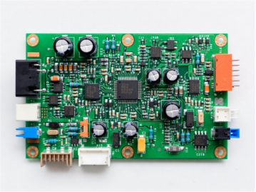
The lid is an unforgiving gauge. Suppose your assembled board works on the bench, then a connector shell catches on the enclosure as you lower it onto the posts. You might suspect the connector placement first. We'd also check the board thickness: a perfectly acceptable fabrication result can still leave a poorly matched assembly unable to fit. The question is whether your drawing allows a board that the rest of the product cannot accommodate.
The Thickness Range Behind a Nominal Size
A drawing marked “1.6 mm PCB” leaves us a question: how far either side of that figure can the board go? Your enclosure won't accept a board merely because it carries the right nominal size. The fabrication agreement needs an upper and lower limit, with the measured surfaces identified. We cannot infer that agreement from a laminate designation.
The useful PCB thickness tolerance for your build depends on that fit requirement and the proposed construction. At PCBA Store, our work includes rigid PCB fabrication and assembly. Bring us the mechanical limit while we're discussing the board, rather than waiting until populated samples are ready for the enclosure.
The Board You Measure After Lamination
The PCB stack-up explains what goes into the laminated board. Your mechanical drawing answers a different question: how much space may that finished board occupy? We need both. A core substitution might look harmless in the stack-up discussion while changing the dimension on which an enclosure approval depends. Keep the mechanical limit visible during that review.
The measurement location deserves a mark on the drawing. At a card edge, the socket meets a particular finished surface, not an average of readings taken elsewhere. Point to that surface and agree whether the specified measurement includes its coating or plating. Otherwise, you and the inspection team could obtain different readings without either instrument being wrong.
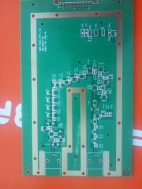
Where the Board Edge Becomes the Mating Part
The socket's accepted thickness is the first figure we'd check for a card-edge design. You are sliding the board between contacts intended for a particular range. Outside it, insertion or contact engagement may suffer. Choosing a familiar connector family won't settle this; the variant in your BOM must match the finished edge you intend to supply.
What Does the Connector Drawing Control?
Look for accepted PCB thickness, mating depth, contact position, bevel, and the edge keep-out. A nominal thickness does not establish those details. If the fingers need a specified finish, keep that note on the fabrication drawing. Changing the layer construction while keeping the same socket is enough reason to reopen the local edge check.
The sample test is straightforward. Put representative boards near the lower and upper agreed limits into the actual connector. Record insertion force by the method your team uses, confirm full seating, and check retention. Do not force a tight sample until it “fits.” A bent contact can give a good bench reading and a poor connection after shipping.
Mounted Connectors Shift the Fit Question
A soldered connector presents a different problem. Its socket may never touch the PCB edge, yet its shell still has to meet a panel opening. We'd trace the dimensions from the surface supporting the board to that shell. If the route crosses the PCB from underside to top, a thickness change moves the connector along that route.
We assemble both through-hole and surface-mount components. Across these PCB connector types used in assembly, the mounting details differ, but a correct footprint alone won't prove panel alignment. We need to see the installed relationship. A section view through the connector and enclosure often explains the problem better than a top-down layout.
For example, take a top-mounted connector on a board supported underneath. A thicker board raises the shell relative to those supports. Now allow for variation in the posts and the panel opening as well. Would the shell still pass through? This is how individually acceptable parts can produce an assembly that binds; no single part has to be defective.

The Enclosure Is a Tolerance Chain, Not a Single Gap
Lid clearance calls for the same calculation, this time ending at the tallest relevant component. Measure from the support plane, through the finished circuit board thickness, to the component top, then compare that height with the lid's inside surface. We'd check the tallest permitted combination against the lowest lid position. The nominal gap can be reassuring and still conceal contact at those limits.
Mounting deserves a look before you tighten anything. If a board rocks on its supports, pulling it flat with screws may bend it rather than correct the underlying mismatch. We'd investigate the support heights and any obstruction underneath. A slotted hole may help with lateral positioning; it cannot lower an assembly that is already too tall.
Interface | Dimension to Confirm | Practical Fit Check |
Card-edge socket | Finished thickness at mating edge | Seat boards near both agreed limits in the specified socket |
Panel connector | Connector position from board mounting datum | Mate through the panel opening with fasteners installed |
Lid clearance | Standoff, board, and component height limits | Close the enclosure on the highest permitted assembly |
Mounting posts | Hole position and support-plane height | Check for rocking before fastening |
The conditions in the right-hand column belong in your fit review. A thickness reading answers one question; seating a connector or closing the lid answers another. Keep the result of each, so a later failure can be traced to the dimension or interface involved.
Measurements That Make a Repeat Build Comparable
The fabrication drawing should identify nominal finished thickness and allowed variation. If the card edge is tighter, call it out at the edge. The mechanical drawing should identify the standoff plane, panel opening, and component envelope. Give both drawings the same board revision. That prevents a new stack-up from being approved while the enclosure team still uses the old number.
Checking the thickness of PCB boards during production belongs with the other agreed dimensional checks. Our fabrication process includes final physical inspection, but an enclosure trial needs a separate arrangement. Tell us which feature is critical and what hardware represents it. We should agree on that work before calling the first article approved.
A short record helps you revisit the approval after a change:
· Identify the board revision and measurement locations.
· Record actual thickness, not only a pass tick.
· Identify the socket, enclosure, and mounting hardware used.
· Recheck affected interfaces after a construction or part change.
Release the Assembly on Fit, Not Appearance
The practical decision is whether boards at the allowed thickness limits still mate and mount correctly. Put the connector's accepted range and the enclosure's height chain beside the fabrication tolerance. If they do not overlap with margin, change the design or the agreed manufacturing limit before volume assembly. A pass on one attractive prototype is not a production fit criterion.
For a build with little room around the board, contact us with the mating-part details and the dimension causing concern. We can discuss that requirement alongside the fabrication and assembly work.
FAQ
Will a Nominal 1.6 mm Board Fit My Socket?
That number alone cannot tell you. We'd compare the socket's accepted range with the lower and upper limits on your finished edge. Matching nominal values is encouraging, but the permitted variation still needs checking.
Which Drawing Needs the Thickness Limits?
Use the fabrication drawing for the finished board limit. Where a card edge has its own requirement, point to it. The enclosure drawing then needs the matching board revision, so its fit calculation uses the same range.
Should We Measure Over the Solder Mask?
Agree on the surfaces first. A reading over mask and one across exposed finished contacts need not be equivalent. For the socket, we're interested in the surface it actually meets; name that location in the inspection requirement.
Why Does a Working Board Fail the Enclosure Check?
The bench test may never involve the enclosure. A board can respond correctly while its connector sits too high for the panel opening. We need the mechanical trial as well, with the supports and mating parts in place.
What Does One Successful Prototype Prove?
It proves that particular combination worked. If its thickness was near nominal, it tells you little about a board at either limit. For a critical interface, include representative limit samples in an agreed validation plan.
Previous article:PCB Cleaning: Flux Removal Before Moisture Protection



