General, quoting & support.
Add: Building E, No.58, Nanchang Road, Xixiang , Baoan District Shenzhen City, Guangdong, China
Tel : 0755-27348887
Fax : 0755-27349876
E-mail : svc@pcbastore.com

PCB Tinning vs Gold Fingers in Assembly
PCBA Store / 2026-11-04
Contents [hide]
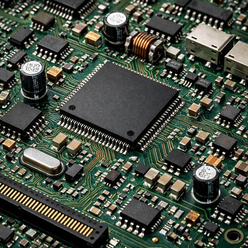
The phrase gold-plated board leaves quite a lot unsaid. Gold on a component pad and gold on an edge finger can serve different purposes, even on the same PCB. For OEM teams comparing PCB tinning with gold fingers, the first task is to identify the connection: a solder joint, a socket contact, or both in separate regions. Only then does a finish specification become useful to production.
Soldered Pads and Mating Contacts
Solder pads spend part of their life waiting for assembly. Their finish protects the metal during that interval and must suit the later soldering operation. Storage therefore belongs in the discussion with wetting and flatness. A board assembled immediately and a board held for a later batch do not present the same handling question.
Edge contacts have to work after assembly, when the board is plugged into its socket. On insertion and withdrawal the surfaces rub. If this will happen repeatedly, the finish needs to be chosen with that wear in mind. Good solderability is useful at a component pad, but it is not a mating-life rating.
A plug-in industrial module may need both surfaces. Label the edge fingers separately from the pads that will receive components. This lets the drawing describe the required solderable finish without accidentally applying it to the socket interface as well.
What PCB Tinning Can Mean
PCB tinning is an imprecise purchasing description unless the process is named. It can refer to adding solder to a surface, a tin-containing hot-air solder leveling finish, or an immersion tin finish. Those processes produce different surfaces. A drawing that simply says tinning leaves room for incompatible interpretations.
Immersion Tin
Immersion tin is one specific option behind the loose term tinning. Specify it by name if it is the intended solderable finish. Before buying boards for later assembly, obtain their handling and storage requirements, and confirm the heat exposures planned for the build. Those limits need an answer for the supplied boards, not a general assumption about tin.
Hot-Air Solder Leveling
HASL leaves solder on the pads through hot-air solder leveling. That is a different process from immersion tin, with a different surface profile. On fine-pitch work, bring the pad-flatness question to the assembler. Also identify the solder alloy; a photograph of a silver surface cannot tell purchasing everything it needs to specify.
The finish decision becomes easier when fabrication and assembly requirements are reviewed together. PCBA Store offers HASL, immersion tin, ENIG, and electroplated gold options. Our PCB tin plating options should be matched to the actual pad function and assembly plan, with the selected process named clearly.
Why Gold Fingers Need Their Own Specification
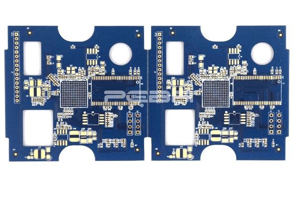
PCB gold fingers identify the edge contacts, but leave the plating details to be specified. Hard gold is an electroplated finish used for wear resistance at such contacts. The thickness and underlying layers still need to be defined. Don't turn the presence of fingers on a drawing into an assumed number of allowable insertions.
ENIG is easily confused with hard gold by appearance. Its full name, electroless nickel immersion gold, describes a different finish used for solderable surfaces. If someone proposes ENIG for an interface originally specified with hard gold, treat that as a design change requiring review. The similar color offers no basis for accepting it.
The socket drawing supplies the other half of the interface. Compare its required board thickness and edge geometry with the PCB, including contact positions and insertion depth. Where the drawings disagree, resolve the dimensions before fabrication. Changing the finish will not make an incorrectly sized edge fit the socket.
Surface or Feature | Main Purpose | Decision to Resolve |
Immersion tin on solder pads | Maintain a solderable surface | Storage, handling, and assembly compatibility |
HASL on solder pads | Provide a solder-coated surface | Alloy and pad-flatness requirements |
ENIG on solder pads | Provide a solderable nickel-gold finish | Compatibility with the intended assembly |
Hard gold on edge fingers | Support a wear-resistant mating contact | Connector requirements and specified plating |
Assembly Can Affect the Contact Area
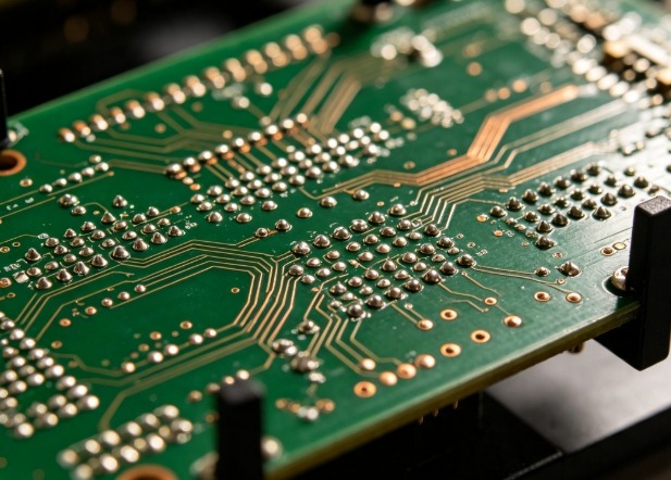
Assembly handling must preserve the mating area. Agree how operators will handle the board and keep solder, residue, and damage away from its fingers. This deserves an explicit instruction when several operations follow fabrication. An acceptable incoming contact surface is of little benefit if later handling leaves it in a questionable condition.
Selective finishes need boundaries that production can follow. Mark the soldered regions and the mating regions, then ask the fabricator to confirm the proposed combination. Use that same marked drawing to review coating instructions. The fingers must remain available to do their job in the connector.
Our work covers SMT, through-hole, and mixed assembly. For PCB gold fingers in assembly, bring the marked finish regions into the process review. We need the proposed combination on the actual drawing before confirming a route. Separate capability listings do not answer whether every finish combination can be made together.
An assembly inspection result has a limited meaning. Checking a solder joint is not a measurement of gold thickness, and powering the board is not a wear test of the socket interface. For a specified plating or mating-life requirement, ask for the corresponding evidence. Do not infer it from a list containing AOI, X-ray, and functional testing.
A Finish Review That Resolves the Ambiguity
The review should end with an agreed drawing. Work through the solder pad assembly requirements and the socket requirements using the same revision. Resolve the shared issues, including handling and selective finishing, before release. Purchasing can then order against a defined combination instead of negotiating the meaning of tinning afterward.
Before releasing the board, resolve these points:
· The exact finish process for solder pads and mating contacts.
· The connector drawing and the required board-edge geometry.
· Any specified plating layers, thicknesses, and acceptance evidence.
· Storage, handling, and thermal-cycle limits relevant to assembly.
· Areas that must remain free of solder or protective coatings.
Prototype evaluation needs the intended socket. Try the actual board and connector under the planned evaluation conditions, alongside the assembly checks. A successful first insertion settles only the immediate fit question. Repeated mating, where required, needs its own evidence for the proposed interface.
The Right Finish for Each Job
Each working surface needs a defined process. Keep the solder-pad requirement separate from the mating-contact requirement, then obtain confirmation that they can be manufactured and assembled together. This is the useful outcome of the tinning-versus-gold discussion: an unambiguous board requirement that production can follow.
For a PCBA Store build with both soldered pads and edge contacts, contact us with the proposed finish regions for review before production.
FAQ
Is PCB Tinning the Same as Immersion Tin?
Not reliably. People use tinning for several applications of tin or solder, including processes other than immersion tin. Obtain the exact process name and record it on the drawing or fabrication requirement before ordering.
Can ENIG Replace Hard Gold on Gold Fingers?
It needs review as a proposed change to the interface. The finishes differ, and a similar gold color does not establish equivalent wear performance. Check the connector requirements and evidence for the intended mating duty before accepting the change.
Can a PCB Have Tin-Finished Pads and Gold Fingers?
Ask the fabricator to review that specific combination. Mark the regions clearly and obtain confirmation against the drawing. It is not enough to find tin and gold listed separately among the available finishes.
Should Gold Fingers Be Covered With Solder?
Normally the specified finger surface is the one that should meet the socket contact. Adding solder changes it and may affect fit. Follow the interface design rather than treating extra solder as protection for the gold.
How Many Insertions Will Gold Fingers Survive?
That number needs support for the actual finished board and connector. Plating, contact arrangement, and operating conditions all contribute. Specify the required duty and obtain suitable evidence; there is no insertion count implied simply by the words gold fingers.
Previous article:Component Identification Before PCBA Production



