General, quoting & support.
Add: Building E, No.58, Nanchang Road, Xixiang , Baoan District Shenzhen City, Guangdong, China
Tel : 0755-27348887
Fax : 0755-27349876
E-mail : svc@pcbastore.com

PCBA Testing and Post-Assembly Quality Inspection
PCBA Store / 2026-09-18
Contents [hide]
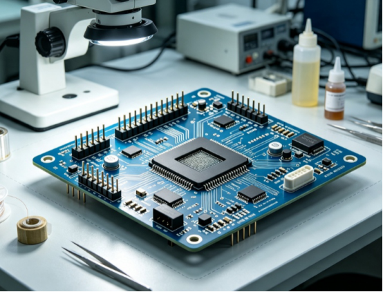
A populated board can look clean and still fail when a polarity error, hidden solder void, wrong component, or weak connection appears under power. PCBA testing is most useful when every method has a defined question, a clear limit, and a documented response when the result is outside tolerance.
Quality Inspection Starts with the Failure Modes
Inspection planning should begin with the ways the board could fail in its real application. A medical controller, robot drive board, industrial sensor, or drone control module may need different emphasis on hidden joints, programming, current draw, communication, or load behavior.
Visual inspection remains valuable because it catches basic conditions early. Operators can identify damaged parts, missing components, lifted leads, obvious solder bridges, contamination, and orientation problems before the board reaches more expensive test stages.
A layered test plan usually includes
· Visual inspection for workmanship, orientation, damage, and obvious omissions.
· AOI for visible solder, paste, placement, missing components, and polarity.
· X-ray for hidden joints and area-array packages.
· ICT or flying probe for selected electrical nets and component conditions.
· Functional testing for the assembled board's intended behavior.
What Each Inspection Method Can Prove
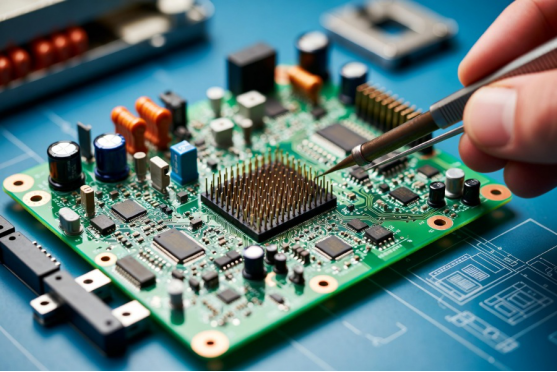
AOI is strongest when the defect is visible and the reference data is accurate. It can compare component presence, placement, polarity, solder shape, and paste-related conditions against the approved program, but it cannot prove that every hidden joint or system function is correct.
X-ray extends coverage beneath packages and around internal features. It is particularly useful for BGA and QFN joints, where opens, shorts, voiding, or abnormal solder formation may not be visible from the board surface.
PCBA Store lists visual inspection, AOI, X-ray, ICT, and functional testing among its testing procedures. Teams building a PCBA quality inspection workflow should map each method to a risk instead of counting test names as proof of coverage.
Inspection method comparison
Method | Best at finding | Main limitation |
Visual inspection | Damage, omissions, polarity marks, and visible workmanship issues. | Cannot judge hidden joints or complete electrical behavior. |
AOI | Visible placement, solder, paste, missing parts, and polarity. | Depends on correct program data and line of sight. |
X-ray | Hidden joints, BGA, QFN, voiding, and internal solder patterns. | Needs interpretation against project limits. |
ICT or flying probe | Selected electrical continuity and component or net checks. | Coverage depends on access, points, and test development. |
Functional test | Whether the board performs its intended operating sequence. | Needs a stable procedure, fixtures, and expected outputs. |
ICT, Flying Probe, and Functional Testing Serve Different Jobs
ICT checks selected electrical conditions through test points or fixture access. It can be efficient for repeatable production when the board, fixture, and coverage have been designed together, but it is not automatically the best fit for every prototype or low-volume build. When testing circuit boards, this method is most useful when the required nets and fixture access are defined in advance.
Flying probe testing uses moving probes instead of a dedicated bed-of-nails fixture. It can reduce fixture investment and adapt to changing boards, although the test time and coverage must be considered against the production quantity and fault risk.
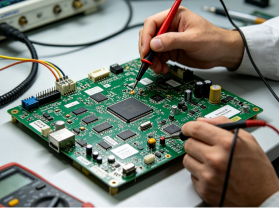
Functional testing answers the system question: does the board respond correctly when power, signals, loads, firmware, or communication are applied? A practical post-assembly testing methods plan defines inputs, outputs, timing, limits, and the operator's response to a failure.
A Test Record Turns Results into Quality Evidence
A useful test record identifies the board revision, lot, serial or panel reference, equipment, program version, operator, date, limits, and result. This information lets a team trace a failure to a design revision, component batch, process change, or test setup.
The record should also separate a failed board from a failed test station. Repeating a test without recording the original symptom can hide intermittent behavior and make corrective action harder. A short failure code and a clear retest rule protect the meaning of the data.
Test limits should be stable enough for production but specific enough to catch drift. A current limit that is too wide may pass a damaged board, while a limit that is too narrow may create false failures. The test owner should review borderline results and update the procedure only through controlled approval.
The production test planning support is most valuable when it connects assembly data with the customer's own acceptance procedure. For professional equipment, the final test should prove the behavior that matters in the finished product, not just that the board receives power.
How Results Should Guide Corrective Action
A failed AOI result should lead first to a visible assembly review, while an X-ray anomaly may require solder profile, stencil, pad, or component analysis. A functional failure may point to assembly, programming, firmware, fixture, or upstream design conditions. These steps form part of practical circuit board diagnostics because each symptom points to a different cause.
Root-cause work becomes faster when the test stages are linked. If a relay does not switch, the team can compare polarity, solder joints, coil resistance, drive voltage, and load behavior instead of treating the symptom as one generic PCBA defect.
Professional acceptance should be written before production. IPC-A-610 is commonly used as a workmanship reference, while project drawings, safety limits, and functional requirements define the additional conditions that are specific to the product.
The Practical Takeaway for PCBA Testing
Reliable post-assembly inspection is a chain of evidence. Visual checks find basic issues, AOI and X-ray extend physical coverage, electrical tests examine selected nets, and functional testing confirms the board's real behavior.
The next sensible action is to list the board's high-risk components and functions, then assign each one a test method and an acceptance limit. That small matrix usually exposes gaps before the first production lot is released.
When the test plan needs to be matched to a new board, contact PCBA Store with the approved files, test procedure, and any special inspection criteria so the required coverage can be discussed early.
FAQ
What is PCBA testing?
PCBA testing verifies whether an assembled printed circuit board meets physical, electrical, and functional requirements. It can include visual inspection, AOI, X-ray, ICT, flying probe, and functional testing.
Is AOI enough for a completed PCBA?
No. AOI is useful for visible defects, but it cannot prove hidden solder joints or full electrical behavior. The final plan should add the methods required by the board's actual risks.
When should X-ray inspection be used?
X-ray is useful for hidden solder joints and packages such as BGA and QFN. It can support investigation of opens, shorts, voids, and unusual solder patterns.
What is the difference between ICT and functional testing?
ICT checks selected electrical conditions at accessible points, while functional testing runs the board in a way that reflects its intended operating behavior.
What should a PCBA test record contain?
A useful record includes the board revision, lot or serial reference, equipment and program, limits, result, operator, date, and a traceable failure or retest code.



