General, quoting & support.
Add: Building E, No.58, Nanchang Road, Xixiang , Baoan District Shenzhen City, Guangdong, China
Tel : 0755-27348887
Fax : 0755-27349876
E-mail : svc@pcbastore.com
What are Bare and Zero PCBs
PCBA Store / 2025-09-25
Contents [hide]
Printed Circuit Boards (PCBs) are the essential foundation of nearly every electronic gadget. Among the different kinds of PCBs, two terms often come up: Bare PCB and Zero PCB. Each has a unique role in the world of electronics design and production. Knowing what sets them apart, along with their build and purpose, is vital for engineers, hobbyists, and manufacturers.
What is a Bare PCB?
Definition and Basic Structure of a Bare PCB
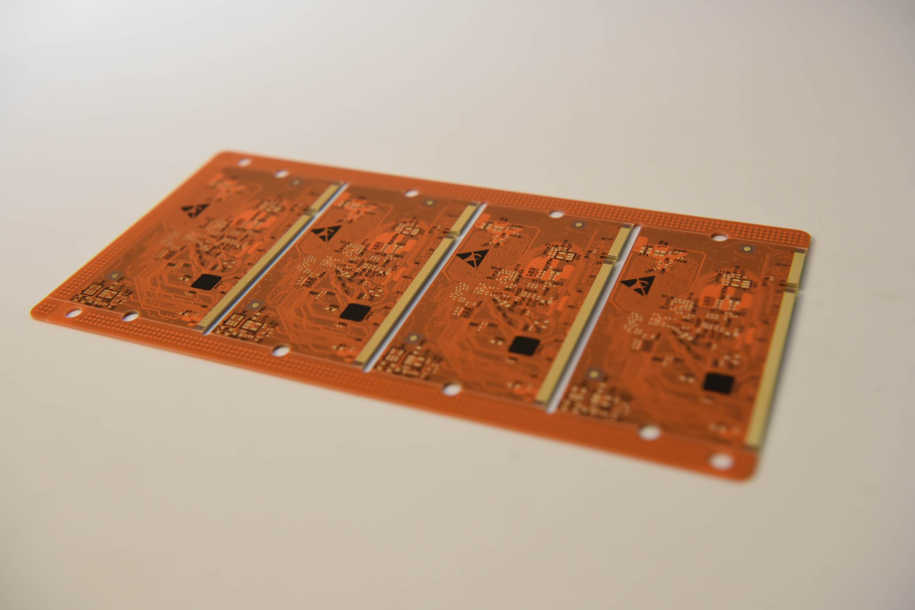
A bare PCB, sometimes called a blank PCB, is a printed circuit board without any electronic parts attached. It’s made up of just the basic materials that create the board’s framework and electrical routes. These materials often include a base layer (like FR4), copper traces for carrying current, a solder mask to shield the copper from rust, and a silkscreen layer to mark where parts go.

Without any components, though, the bare board only offers electrical paths. It lacks the ability to work as intended. Basically, it’s an unfinished piece that needs further steps, like soldering and assembly, to become useful.
Key Characteristics of Bare PCBs
The main traits of bare PCBs are:
· No electronic parts are attached.
· They have copper traces for conducting electricity.
· They might include a solder mask and silkscreen.
· They need testing before assembly begins.
Bare PCBs are like a blank slate where working circuits are crafted. Their quality plays a big role in how well the final electronic item performs and lasts.
Common Applications of Bare PCBs
Bare PCBs are found in many fields, such as car electronics, medical tools, factory control systems, communication devices, and everyday gadgets. They’re the starting point for everything from basic LED setups to advanced multilayer boards used in aerospace tech.
Bare Board Testing
Purpose and Importance of Bare Board Testing
Checking bare boards is a must before adding any parts. It’s important to confirm that the electrical connections are solid. Issues like shorts or broken circuits can make a board useless or lead to failures in important uses.
Many flaws, like shorts or gaps, can’t be spotted just by looking. That’s why special electrical tests are used to make sure everything is reliable.
Types of Testing Methods Used
Electrical Continuity Testing
This test checks if all planned connections on a PCB are working right. It makes sure electricity can move through the set paths without any breaks.
Isolation Testing
Isolation testing looks for unwanted connections, or shorts, between separate paths. This helps avoid issues like cross-talk or electrical mix-ups between circuits.
To check the electrical setup on a bare board, two popular ways are the flying probe test and the fixture test.
The flying probe test uses movable probes with driving tools to touch test pads and vias on the board. This approach is handy for various designs since it doesn’t need custom setups.
The fixture test, on the other hand, uses a specific test setup with many probes that match the PCB’s nets exactly. It’s faster and better for large-scale production, but it’s less adaptable than flying probes.
Equipment Used in Bare Board Testing
Testing tools include flying probe testers for flexible checks and bed-of-nails fixtures for big-batch testing. Other devices, like AOI (Automated Optical Inspection) machines, might also be used early on for visual checks.
What is a Zero PCB?

Understanding the Concept of Zero PCBs
A Zero PCB, also known as a Perfboard or DOT PCB, is a board that isn’t made for one specific job or purpose. Instead, it’s a flexible, general-use board. It has evenly spaced holes set in a grid layout. Each hole stands alone electrically unless linked by wires or solder bridges by hand.
Differences Between Zero PCBs and Standard PCBs
Unlike standard PCBs that come with set circuit designs for specific tasks:
· Zero PCBs have tiny holes in a grid, each one separate from the others electrically.
· They don’t have preset traces or nets.
· They don’t come with automated design files like Gerbers.
· Users need to connect parts by hand during testing or trial phases.
The word ‘zero’ here means there are no built-in connections, layouts, or set roles on the PCB.
Use Cases for Zero PCBs in Prototyping
Zero PCBs are perfect for:
· DIY electronics crafts
· Learning and school projects
· Quick trial designs
· Testing basic ideas
They let engineers play around with ideas without spending on full production right away.
Copper Traces or Pads
Role of Copper Traces in PCB Functionality
Copper traces act as pathways that carry electricity to connect different parts on a circuit board. Whether it’s sending power or signals between ICs (Integrated Circuits), resistors, capacitors, or other bits, these traces control how electricity moves in a device.
In Zero PCBs, these copper bits offer paths for soldering parts and making links.
But, on Zero PCBs, the copper traces usually aren’t joined. This gives users total control to set up their circuits by wiring them manually.
Design Considerations for Copper Pads and Traces
Trace Width and Spacing Guidelines
The width of traces must handle the needed current flow, while spacing keeps shorts from happening by mistake. Common rules often suggest minimum trace widths based on current needs using IPC-2221 standards.
Pad Size and Placement
Pad sizes should match the leads or pins of parts while having enough area for strong solder joins. Good placement makes things easier for both hand soldering in prototypes and machine placement in production.
No Solder Mask and Silkscreen
Explanation of Solder Mask and Its Absence in Certain PCBs
A solder mask is usually put over copper traces to stop rust and prevent accidental links while soldering. However, Zero PCBs often don’t have a solder mask.
Not having it means users can freely reach the copper areas, but it raises the chance of shorts if they’re not careful while putting things together.
Impact of Not Having a Silkscreen Layer on Assembly and Usage
Silkscreen layers show labels for parts (like R1 for resistor 1). Without this layer, as is common in most Zero PCBs, users must keep track of placements using diagrams or notes. This can lead to mistakes while building or fixing things.
Because of this, Zero PCBs are kept basic in design. They focus on being flexible rather than guiding assembly.
Advantages and Limitations of Excluding These Layers
Advantages:
· Cheaper to make
· More freedom during testing phases
· Easier board-making process
Limitations:
· Greater risk when soldering by hand
· No helpful markings to guide
· More time needed to track parts and connections manually
FAQ
Q: Can I use bare PCBs right out of the box?
No. A bare PCB doesn’t have parts on it. It needs assembly before it can work electrically.
Q: Are Zero PCBs reusable?
Usually not. Once parts are soldered on by hand, reusing them is tough due to fixed wiring unless you carefully remove the solder.
Q: Which is better—bare PCB or Zero PCB—for beginners?
Zero PCBs are more flexible for learning how to design circuits hands-on. You don’t need fancy tools or production services to start.
Q: Do Zero PCBs support surface-mount technology (SMT)?
Not really. Most Zero PCBs are made for through-hole parts. SMT needs special pads, which these boards usually don’t have unless users tweak them creatively.
Get Your Instant PCB Quote from PCBAStore
If you’re moving from early designs with Zero PCBs to full production with custom bare boards, PCBAStore has complete solutions, including making and assembling boards.
From PCB design and layout to prototyping, large-scale production, and assembly, our Printed Circuit Boards are used in robotics, medical tools, cars, and everyday gadgets.
With over 16 years of know-how in creating top-notch printed circuit boards at fair prices, and with fast shipping options, PCBAStore is your reliable all-in-one partner.


