General, quoting & support.
Add: Building E, No.58, Nanchang Road, Xixiang , Baoan District Shenzhen City, Guangdong, China
Tel : 0755-27348887
Fax : 0755-27349876
E-mail : svc@pcbastore.com
What Inspection Methods are often used in PCB Aseembly
Byron / 2018-01-09
Contents [hide]

Inspection is crucial to ensure high quality products are delivered to customers. Few things are more frustrating to a customer than an ‘out-of-box’ or premature failure due to an avoidable fault. Thankfully board assemblers offer multiple layers of testing and inspection to ensure high quality units are produced and delivered to customers. Here you can learn some PCB inspection methods often used in PCB Assembly.
1)Visual Inspection
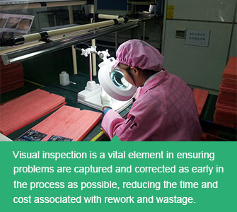
Visual inspection is a vital element in ensuring problems are captured and corrected as early in the process as possible, reducing the time and cost associated with rework and wastage. Which can be used after lots of steps during PCB assembly process and equipment for visual inspection is selected based on the positions of inspection targets. For example, after solder paste printing and device placement, inspection staff is able to find out obvious defects with naked eyes such as contaminative solder paste and missing components. The most prevalent visual inspection is capable of inspecting reflow solder joints by observing light rays reflected from ordinary prism from different angles. Generally speaking, this type of inspection can test 5 joints in just one second.2, Structural Process Test System (SPTS)

• AOI system(AUTOMATED OPTICAL INSPECTION)
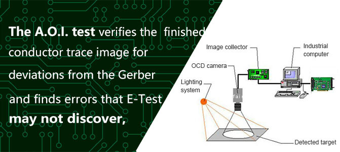
The A.O.I. test verifies the finished conductor trace image for deviations from the Gerber data and finds errors that the E-Test may not discover, such as (for example) narrowed, but still unbroken conductor traces.
The A.O.I. test is especially important for the following application areas:
■High frequency
■High power loads
■High data transmission rates
■Op-amps with high amplification factors and input resistances
The inner layers of multilayer boards are checked using A.O.I. before they are pressed together. This guarantees the high reliability of Multi PCB multilayer circuit boards.

• Automatic Laser Test (ALT) Measurement
ALT is a more direct technology used to test height and shape of solder joints or solder paste deposition. This system runs to measure the height and reflectivity of some surface components when the image of laser beam focuses on one or multiple position sensitive detectors that maintain a certain angle with laser beam. During ALT measurement, surface height is determined by the light position reflected from position sensitive detectors while surface reflectivity is figured out from the power of reflected light beam. Due to secondary reflection, light beam perhaps shines on position sensitive detectors at multiple positions, which calls for a scheme to distinguish correct measurement. Furthermore, reflected light beam may suffer from shielding or interference of interference material when running along light of position sensitive detectors. In order to eliminate multiple reflections and prevent shielding, this system should test reflected laser beam along regulated independent optical path. During multiple height measurement for solder joints, ALT system is OPTIMALfor solder paste deposition quantity and position alignment
prior to component assembly. It provides data for real-time structural process control of solder paste printing including viscosity, alignment, cleanliness, fluidity and squeezing speed and stress.
• X-ray Inspection System
X-ray inspection technology, usually referred to Automated X-ray inspection (AXI), is a technology used to inspect the hidden features of target objects or products with X-rays as its source. Nowadays, X-ray inspection is widely used in lots of applications such as medical, industrial control, and aerospace. As for PCB inspection, X-ray is massively used in the process of PCB assembly in order to test the quality of PCBs, which is one of the most important steps for quality-oriented PCB manufacturers.
In order to get improved industry standard, PCBASTORE have equipped with advanced inspection system and professional staffs to ensure high quality of PCB assembly.
If you have any comments or suggestions about this post, please leave a reply here


