General, quoting & support.
Add: Building E, No.58, Nanchang Road, Xixiang , Baoan District Shenzhen City, Guangdong, China
Tel : 0755-27348887
Fax : 0755-27349876
E-mail : svc@pcbastore.com

When SMT Meets Through-Hole Parts
PCBA Store / 2026-11-13
Contents [hide]
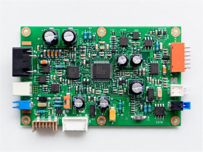
Place a tall connector beside fine-pitch parts and assembly access becomes a design issue. The connector may bear cable loads or block a solder nozzle; heat tolerance can rule out another oven pass.
Components That Determine the Build Order
Mark the THT parts on the drawing and ask what each one needs from its leaded joint. A power connector may need mechanical retention; a tall component may block a nozzle or wave path. Those are different constraints.
A board carrying both package types needs more than two counts on a quote. Our mixed technology PCB assembly services at PCBA Store cover SMT and THT work; the drawing still has to tell us how the two populations share space and which parts can tolerate each heat cycle.
DIP is a package description, not a catch-all for leaded parts. A BOM may also contain THT connectors, relays or inductors. If your drawing calls the whole population “SMT and DIP,” clarify that shorthand. Otherwise the insertion work being discussed may not match the parts actually on the board.
Three Common Routes Through the Line
SMT first and THT afterward is a common route. Reflow the surface-mount population, then fit the leaded parts. The next question is underneath: can the later soldering step reach those leads without exposing or damaging nearby SMT joints? The sequence is workable only when that second operation has room.
Parts That Cannot Follow the Oven Route
The connector housing can rule out an oven pass. Check whether its processing rating covers full-body reflow or only the intended THT solder operation. If it cannot tolerate reflow, installing it after SMT is a constraint on the build. A cheaper sequence cannot change that rating.
Double-sided SMT adds another thermal pass. The second profile must account for parts already attached underneath, especially heavier parts that could shift or lose support. THT insertion comes after that decision.
Pin-in-paste is worth checking when the lead and plated hole suit the available paste volume. Paste goes at the hole, the component is inserted, and reflow forms the joint. Board thickness and lead geometry decide whether it works.
Hole Filling Needs Enough Solder
Pin-in-paste needs a volume check. The lead takes up space inside the hole, while printed paste loses volume as flux leaves during reflow. Enough solder must remain to form the required joint. Give the process engineer the lead, hole and board dimensions; the route name alone settles none of this.
Package choice matters more than a broad component label. A “large connector” is not automatically THT, and a high-current function is not proof that SMT is unsuitable. Review the selected part and its retention needs. Surface-mount alternatives exist, but changing to one is a design decision, not a factory shortcut.
Soldering Access Under the Board
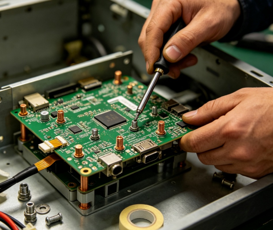
Wave access depends on the underside layout. Draw the wave path through the proposed board and identify what it would touch. Components that must stay clear need protection or a different route. Discuss the pallet and direction of travel with that geometry visible, rather than after the layout is released.
A selective nozzle needs room even when the solder stays local. A neighboring part might avoid direct solder contact yet still block the nozzle body. Check access around the pins before committing the layout; then check whether the thermal mass can be soldered within the permitted exposure.
Hand soldering may be the practical answer for a prototype or an awkward joint. Name those joints in the work plan and agree acceptance. If a later production lot moves them to a machine process, review the change. The thermal exposure and access conditions will not necessarily match the manual operation.
For the assembly of through-hole components, PCBA Store can discuss THT and hybrid builds. Confirm the soldering method for this particular layout. Our general assembly offer should not be taken to mean that every board fits every wave or selective process.
Assembly Details the Placement File Cannot Show
The placement file leaves several decisions unresolved. Use the assembly drawing to make these visible:
· Connector orientation and polarity on both board sides.
· Lead projection or clearance limits that affect the solder tool.
· Parts installed after cleaning or coating, with exclusions identified.
The drawing should call out solder alloy, coating exclusions and test access. If the sequence could go either way, state the preferred order before the assembler plans a route.
An assembly note works better when it explains the restriction. “Install connector last: probe access required” tells the team what must be preserved. “Install last” alone leaves the reason open to interpretation. If the fixture changes later, the first note gives an engineer a basis for reviewing the sequence.
Route Choices for a Mixed Board
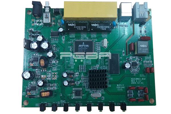
Route | Useful when | Main design checks |
SMT then selective solder | THT joints are localized among bottom-side SMT parts | Nozzle access, thermal exposure, support, joint inspection |
SMT then wave solder | Many compatible THT joints can be processed together | Wave direction, pallet, keep-outs, component orientation |
Pin-in-paste reflow | Lead and hole geometry support paste filling and reflow | Paste volume, lead fit, hole design, thermal profile |
Manual insertion/solder | Low volume or inaccessible parts need controlled placement | Work instructions, labor, inspection, repeatability |
The real layout gets the final say. A theoretically neat route can fail on one blocked nozzle path.
Connector Loads and Joint Inspection
Cable loads can reach the PCB through a connector body and its leads. In an industrial controller or drone assembly, review the support and strain relief as well as the solder joints. More solder is not a substitute for a mechanical load path.
We offer AOI, X-ray and functional testing to your procedure at PCBA Store. Match the method to the question. Is the concern visible placement, a hidden joint, or circuit behavior? A tidy-looking connector and a successful power-on check answer different questions; neither establishes every aspect of the joint.
A Sequence That Fits the Actual Board
Before releasing files, compare the revision printed on the BOM, centroid data and assembly drawing. Same revision? Then settle the solder route, panel and test steps. A mismatch can stop a build at intake.
The finished process plan should identify each thermal pass and the access needed at the THT parts. Revisit both if the route changes. That gives your team something concrete to accept, rather than a generic statement that the board will receive mixed assembly.
For a crowded underside, ask PCBA Store about a selective soldering compatibility review. Treat it as a project-specific feasibility discussion. A hybrid-assembly offer by itself does not identify the machine, nozzle or route that would be used.
For help reviewing the mixed-build sequence, contact PCBA Store with both assembly sides and any component temperature restrictions. We can clarify the proposed SMT and THT scope before you release the order.
Frequently Asked Questions
Should SMT or Through-Hole Components Be Installed First?
Usually SMT is completed first, leaving taller or heat-sensitive THT parts for later. Double-sided placement and component temperature ratings can alter that order, so confirm it against the actual BOM.
When Is Selective Soldering Useful?
It is useful when only selected pins need solder and nearby SMT parts should avoid a full wave. Check nozzle clearance first; localized heating does not remove the access problem.
Can Every THT Part Use Pin-In-Paste?
No. The component must tolerate reflow, and its lead-and-hole geometry must work with the available paste. Those conditions need validation for the intended board thickness.
Does a Mixed Board Always Need Two Soldering Processes?
Not necessarily. A compatible pin-in-paste design may combine operations. Other boards need reflow followed by THT soldering. Count the actual steps after reviewing the packages.
What Should Be Sent for a Mixed-Technology Quote?
Send both assembly sides with the BOM and placement data. Highlight thermal limits, connector orientation and any joint that needs an unusual inspection. Those details explain the work behind the THT count.



