General, quoting & support.
Add: Building E, No.58, Nanchang Road, Xixiang , Baoan District Shenzhen City, Guangdong, China
Tel : 0755-27348887
Fax : 0755-27349876
E-mail : svc@pcbastore.com
A step-by-step guide to building a standard rigid, multi-layer PCB
PCBA Store / 2026-01-16
Contents [hide]
The process of making printed circuit boards (PCBs) goes from basic single-layer types to advanced high-density interconnect (HDI) and flexible ones. Standard rigid multi-layer PCBs serve as the main base for most electronic products. They offer a good mix of performance, dependability, and reasonable cost. This guide walks through the full steps to make a standard rigid multi-layer PCB, starting from customer design files all the way to ready boards. It points out the main stages, common materials, and important quality checks needed to create solid multi-layer boards with plated through-holes.

PCBA Store, a leading PCB manufacturer and PCBA supplier based in Shenzhen, China, offers complete turnkey services for prototypes as well as large-scale production. They make sure of high quality by handling both fabrication and assembly in the same place.
From Customer Files to Manufacturing Data
Customers send design files in formats like Gerber (RS-274X), ODB++, or IPC-2581. Gerber is still the most common choice. Yet IPC-2581 is becoming more popular because it carries more complete information. Once files arrive, the engineering team does a careful check for manufacturability (DFM analysis). Problems such as too-small clearances, missing drill details, or unusual specs get quick feedback. This helps avoid hold-ups later in production.
Base materials get chosen according to what the project needs. FR-4 works as the usual substrate for most rigid multi-layer PCBs. It gives strong electrical insulation, good mechanical strength, and fair pricing. Panels come in common sizes that help production run smoothly. Stackup design sets the final board thickness. It includes copper foil weights (often 1 oz for outer and inner layers), core laminates (cured resin-glass with copper), and prepreg sheets (uncured resin-soaked glass fabric used for bonding).
Manufacturing travelers go with each panel. They record specs, materials, routing info, and inspection points. Default rules follow IPC Class 2 unless the customer asks for Class 3 in cases that need higher reliability.
Inner-Layer Processing: Develop, Etch, and Strip
Inner-layer cores start with cleaning through an acid dip that clears away dirt. Next comes photoresist coating, spread evenly on both sides. The circuit pattern gets transferred using UV light through the phototool or direct imaging. This hardens the resist in the right spots.
Development washes away the unexposed resist and leaves copper open for etching. Ferric chloride or similar alkaline etchants carefully remove extra copper. The resist protects the wanted circuit pattern. Then resist stripping finishes the step and shows clean copper traces.
Automated optical inspection (AOI) checks every inner layer closely. It looks for issues like opens, shorts, or wrong trace widths. Cross-section checks confirm copper thickness and quality. Panels hold several boards together to make processing more efficient.

Lamination
Oxide treatment roughens the copper on inner layers. This improves how well they stick during lamination. Layers stack up exactly as shown in the approved stackup, with prepreg sheets placed between them. The whole stack goes into a hydraulic press. There it gets controlled heat and pressure in set cycles. This cures the resin and bonds all layers into one firm multi-layer panel.
Alignment pins and X-ray registration keep layers lined up correctly before pressing starts. After lamination, inspection checks bond strength and overall thickness.
Drilling and Cleaning Holes for Copper Plating
Precise drilling makes vias and component holes. X-ray drilling finds targets so holes line up well through all layers. High-speed CNC drills create the holes. Care is taken to avoid too much heat that might smear resin.
Desmear or plasma etchback cleans the hole walls. It removes leftover resin so plating works reliably. Electroless copper puts down a thin conductive seed layer first. Then electrolytic plating builds up the needed copper thickness (usually 1 oz in holes). This creates good electrical connections between layers.
Outer-Layer Processing
Outer layers go through a similar develop-etch-strip process like the inner ones. Extra steps include applying dry film resist, exposing the pattern, etching, and stripping. These form the final copper patterns on the outside surfaces.
Solder Mask and Silkscreen
Liquid photoimageable solder mask gets spread over the whole board. It covers pads and vias while it shields the traces. UV exposure and development create the openings. Thermal curing makes the mask tough enough for soldering.
Silkscreen (legend) printing adds component labels, logos, polarity signs, and other markings. Inkjet or screen methods apply it. White or yellow legend ink gives clear contrast against the board.
Final Inspection
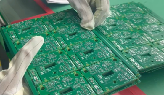
Boards go through strict quality checks. Dimensional inspection uses C=0 sampling to confirm hole positions, tolerances, and overall sizes. Electrical testing (flying probe or fixture-based) verifies continuity and isolation as the customer wants.
One hundred percent visual inspection looks at overall workmanship, solder mask coverage, legend readability, and surface cleanliness. Other tests like impedance control checks or microsection analysis happen for important applications.
Summary
Building a standard rigid multi-layer PCB needs careful work across many specialized steps. Mistakes early on can cause big problems later, leading to wasted boards or ones that fail specs. Working with a skilled manufacturer that has modern tools, certified methods, and strong quality controls reduces risks. It helps get steady results for prototypes and big production runs alike.
PCBA Store supplies dependable standard rigid multi-layer PCBs along with advanced options. These include up to 40 layers in regular production (64 in samples), FR-4 and high-performance materials, minimum trace/space down to 2.5mil/2.5mil, and complete turnkey PCB assembly services. With more than 16 years in PCB fabrication and 8 years in assembly, PCBA Store brings competitive pricing, quick turnarounds (as fast as 24 hours for prototypes), ISO9001:2015 certification, and 99% on-time delivery to support electronics projects around the world.
FAQ
What file formats does PCBA Store accept for PCB fabrication and assembly?
PCBA Store accepts standard Gerber files (RS-274X), ODB++, IPC-2581, drill files, BOM, and pick-and-place data. Upload directly through the online quote system or email to svc@pcbastore.com for manual review.
What are the typical lead times for standard rigid multi-layer PCBs?
Prototype lead times start at 1-10 days, with express options as fast as 24 hours. Production runs depend on complexity and quantity, often 7-15 days standard, with urgent services available.
Does PCBA Store offer turnkey PCB assembly?
Yes. PCBA Store provides full turnkey services, including component sourcing, SMT, THT, mixed assembly, conformal coating, and box-build. No minimum order quantity applies, with options for consigned/kitted parts.
What quality standards does PCBA Store follow?
Manufacturing adheres to IPC Class 2 (default) or Class 3 upon request. Assembly follows IPC-A-610F. AOI, X-ray, functional testing, and 100% visual inspection ensure high yields exceeding 99.5%.
Are there any minimum order quantities or setup fees?
No MOQ exists for fabrication or assembly. No setup charges or NRE fees apply for standard services.
Partner with PCBA Store for Your Next PCB Project
PCBA Store works as a direct manufacturer and supplier with in-house fabrication and assembly facilities in Shenzhen. Businesses gain from smooth one-stop solutions, lower costs without middlemen, fast prototyping, production that scales up, and dedicated engineering help.
Get started today: Visit https://www.pcbastore.com/online_quote.html for an instant online quote, or email design files and requirements to svc@pcbastore.com. Track orders in real time, chat with support 24/7, and enjoy secure payments plus full after-sales protection including refunds or free rework for any quality issues. Contact the team to talk about project needs and get expert advice on stackup, materials, and assembly choices.


