General, quoting & support.
Add: Building E, No.58, Nanchang Road, Xixiang , Baoan District Shenzhen City, Guangdong, China
Tel : 0755-27348887
Fax : 0755-27349876
E-mail : svc@pcbastore.com

Double-Sided Mixed-Technology PCB Assembly Guide
PCBA Store / 2026-09-16
Contents [hide]
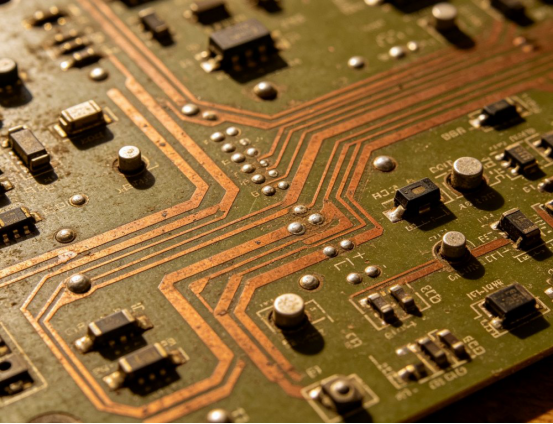
A double-sided board becomes difficult when fine-pitch SMT, larger packages, connectors, and through-hole parts share the same panel. The hard part is not filling two faces. It is keeping the first face stable while the second one is printed, placed, soldered, inspected, and moved through the line.
The Real Challenge Behind Two-Sided Assembly
Two-sided placement creates interaction between thermal cycles and mechanical support. A heavy part on the first face can change how the panel rests on a fixture, while a small part on the second face may see heat or handling that was never considered on its own.
Mixed technology makes the route less forgiving. Controllers and passives need surface-mount accuracy, but connectors, relays, and loaded terminals also need through-hole strength and enough access for soldering and inspection.
Questions that should be answered before release
· Which side carries the densest or heaviest components?
· Which joints need reflow, selective handling, or through-hole soldering?
· Where will supports, fiducials, test points, and inspection access be placed?
· Will the finished board face vibration, heat, repeated insertion, or service handling?
A simple two-layer board may tolerate a routine route that would be risky on a dense industrial controller, medical instrument, robot module, or drone control unit. The process has to follow the actual component mix and the consequence of a weak joint.
How Process Order Protects Both Sides of the Board
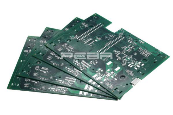
Process order works best when it follows component security and board support. A common route prints and places the more complex SMT side first, reflows it, and then processes the second face with support and temperature control that protect the finished joints.
Component mass and package geometry decide whether a part can remain underneath during another reflow. Large or mechanically sensitive parts may call for adhesive support, selective soldering, a different sequence, or a design change before volume production.
PCBA Store supports SMT, through-hole, and hybrid assembly with single- or double-sided placement. For a team checking its route, the double-sided assembly process details provide a useful starting point for matching the board to the available assembly options.
Process choices by board condition
Board condition | Main risk | Planning response |
Dense SMT on both sides | Paste, placement, and thermal variation can interact across cycles. | Review component mass, support, and reflow order together. |
SMT plus through-hole | THT parts may require a separate soldering step or access plan. | Reserve clear soldering and inspection access around leads and connectors. |
Heavy connectors or relays | Weight can affect support and joint stress. | Check fixture contact points and mechanical retention. |
Fine-pitch or BGA packages | Hidden or closely spaced joints are harder to verify. | Define stencil, X-ray, and rework criteria before release. |
Soldering Decisions Shape Yield and Serviceability
Soldering method has to match the joint, the board, and the use case. Reflow suits surface-mount parts when paste volume and thermal profiling are controlled. Through-hole joints may need wave, selective, or hand soldering depending on access and geometry. Double-sided PCB soldering also needs a sequence that protects completed joints on the first face.
Lead-free and leaded processes also require clear separation in materials, profiles, and acceptance criteria. A board intended for professional equipment should not rely on an informal substitution because solder alloy, finish, thermal mass, and component limits can change the result.
Stencil design becomes especially important when one side mixes small passives with larger pads. A uniform aperture rule can overprint some joints and underprint others. Local aperture adjustments, paste inspection, and a thermal profile tied to the board stack-up provide better control than a single generic recipe.

Inspection Has to Follow the Technology Mix
Inspection is useful only when it answers the board's likely failure questions. AOI can check visible solder, placement, missing parts, and polarity. X-ray reaches hidden joints such as BGA and QFN packages. Functional testing then shows whether the assembled board performs its intended task.
PCBA Store describes AOI, X-ray, and functional testing as different parts of its quality process. Buyers comparing mixed-technology production capabilities should ask how each method is assigned to the board's actual risks rather than treating inspection as one undifferentiated step.
Acceptance criteria should be agreed before the build. Many professional programs use IPC-A-610 as a reference for electronic assembly acceptability, but the project still needs its own drawings, critical-to-function limits, and test procedure where the general standard does not describe the full product requirement.
The inspection plan should also account for what happens after shipment. Boards that will be serviced in the field may need accessible test points, clear revision markings, and a rework route that does not disturb the opposite side. That small amount of planning can reduce the cost of diagnosing a two-sided assembly later.
Data and Fixtures Keep the Second Side Predictable
A complete data package removes many avoidable stops. The BOM, Gerber or other PCB files, Pick-and-Place data, drawings, polarity information, and approved substitutions need to describe the same revision and orientation.
Fixtures matter because a board can flex when one side is already populated. Support points should avoid sensitive parts, connectors, and solder joints while still keeping the panel stable for printing, placement, inspection, and test.
For industrial, medical, robotic, and drone electronics, a stable fixture and a clear revision record also make rework easier to trace. The PCB assembly service for both sides can be a useful reference when the build needs fabrication, assembly, and testing decisions to stay connected.
The Practical Takeaway for Mixed Technology Boards
Reliable double-sided mixed-technology assembly comes from treating both faces as one process. The design team and assembly partner should agree on sequence, support, soldering method, inspection coverage, test access, and rework before the board reaches the line. For double-sided mixed PCB assembly services, that means coordinating both faces before the board reaches the line.
A useful next step is to mark the heaviest components, the densest footprints, the hidden joints, and the mechanically loaded connectors on the approved layout. Those four markings quickly reveal where process order and inspection need the most attention.
When the board needs a production review, contact us with the current BOM, PCB files, Pick-and-Place data, and any special soldering or test requirements so the process can be evaluated against the actual assembly mix.
FAQ
What is double-sided PCB assembly?
Double-sided PCB assembly places components on both faces of a board. The process must control printing, placement, soldering, support, and inspection across multiple operations.
What makes mixed-technology assembly different?
Mixed-technology assembly combines SMT with through-hole parts, so the board needs different placement, soldering, access, and inspection decisions within one production flow.
Can both sides of a PCB go through reflow?
Many designs use more than one reflow cycle, but the sequence depends on component mass, package limits, board support, and the risk of disturbing the first side.
When is X-ray inspection useful on a two-sided board?
X-ray is useful when packages hide their joints or when the board contains BGA, QFN, or other features that cannot be fully judged from the top surface.
What files are needed for a double-sided assembly quote?
A typical package includes the BOM, Gerber or other PCB files, Pick-and-Place data, drawings, and notes covering polarity, orientation, substitutions, soldering, and testing.
Previous article:China Turnkey PCB Assembly for Global OEMs



