General, quoting & support.
Add: Building E, No.58, Nanchang Road, Xixiang , Baoan District Shenzhen City, Guangdong, China
Tel : 0755-27348887
Fax : 0755-27349876
E-mail : svc@pcbastore.com

PCB Assembly Testing Methods: ICT, Flying Probe and Functional Test
PCBA Store / 2026-07-08
Contents [hide]
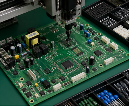
In global electronics supply chains, PCB Assembly quality is no longer verified only at the final shipment stage. B2B buyers now expect structured testing across production to reduce failure risk and ensure stable long-term performance. At PCBA Store, we integrate multiple PCB testing methods into our manufacturing process in China to support consistent quality control and scalable production.
This article focuses on three key circuit board testing methods and how they are applied in real PCB Assembly workflows to improve reliability and reduce supply chain risk.
PCB Assembly Testing System in China Manufacturing
PCB Assembly testing is structured as a multi-stage process rather than a single inspection step. Each stage targets different defect types, ensuring issues are identified as early as possible in production.
The main objectives include:
· Detecting electrical defects before final assembly
· Ensuring component placement accuracy
· Verifying circuit continuity and stability
· Reducing failure risk in mass production
This layered approach is essential for OEM and ODM projects where consistency and repeatability are critical.
ICT Test PCB in Mass Production Control
ICT Test PCB is widely used in stable, high-volume PCB Assembly programs. It focuses on electrical verification using a fixed testing system connected through a PCB Test Jig.
Electrical testing through ICT system
The ICT test PCB method uses a jig-based fixture to contact specific test points on the PCB. This allows fast measurement of key electrical parameters.
Core defects detected include:
· Open and short circuits
· Wrong component values
· Soldering defects
· Missing components
Test Item | Function |
Circuit continuity | Detect open/short faults |
Component values | Verify resistance/capacitance |
Assembly errors | Identify missing or wrong parts |
PCB Test Jig Role in ICT
The PCB test jig ensures stable contact and repeatable measurement during mass testing. In high-volume PCB Assembly, jig accuracy directly affects production efficiency and defect detection rate.
However, ICT is most suitable for stable designs because fixture development requires upfront engineering time and cost.
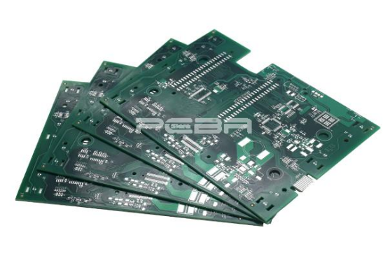
Flying Probe Test for Flexible PCB Assembly Verification
Flying Probe Test is widely used in prototype PCB Assembly and small-batch production where design iterations are frequent and tooling cost must be minimized.
Non-fixture based circuit validation method
The flying probe test uses movable probes instead of fixed jigs. These probes automatically navigate across the PCB surface and contact test points according to programmed coordinates.
This structure removes the need for custom fixtures and allows rapid setup for new PCB designs.
Application in fast-turn PCB manufacturing
Flying probe systems are commonly used in early-stage engineering builds and sample validation. In our PCB Assembly workflow, it supports quick feedback loops between design and manufacturing teams.
Main application scenarios:
· Prototype PCB Assembly validation
· Engineering sample testing
· Low-volume customized production
· Complex multilayer PCB inspection
Performance comparison in production use
Flying probe testing is slower than ICT in mass production, but provides higher flexibility. It is particularly effective for high-mix product environments where multiple PCB versions are processed in parallel.
Method | Setup Time | Volume Suitability | Fixture Required |
Flying Probe Test | Low | Low to medium | No |
ICT Test PCB | High | Medium to high | Yes |
This makes flying probe testing a core part of flexible manufacturing strategies in China-based PCB Assembly facilities.
Functional Test for System-Level PCB Validation
A functional test is used to verify whether a fully assembled PCB performs correctly under real operating conditions. Unlike ICT or flying probe methods, it focuses on system behavior rather than component-level inspection.
Real operating condition simulation
During functional testing, the PCB is powered under controlled conditions to simulate actual usage scenarios. This allows verification of signal processing, power distribution, and output response.
Typical functional test items include:
· Input/output signal response accuracy
· Power stability under load conditions
· Communication interface reliability
· Integrated system behavior consistency
Role in final quality assurance stage
Functional testing is positioned as the final checkpoint in our PCB Assembly process. It ensures that even if component-level tests pass, the system still performs correctly in real applications.
This step is essential for reducing field failure risk in industrial, medical, and consumer electronics applications.
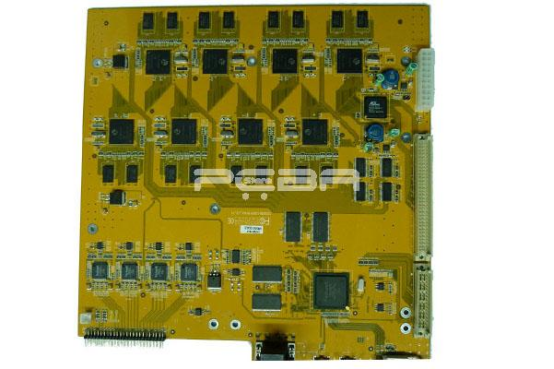
Integrated Circuit Board Testing Methods in PCB Assembly Workflow
We do not treat each testing method independently. Instead, all circuit board testing methods are integrated into a structured production system designed for risk reduction and quality consistency.
Standard workflow structure in our PCB Assembly line:
· Incoming material inspection
· SMT placement verification
· Reflow soldering inspection
· ICT Test PCB for electrical validation
· Flying Probe Test for prototypes and sampling
· Functional Test for system verification
· Final visual inspection and packaging control
This multi-layer system ensures defects are detected at the earliest possible stage rather than at shipment.
Quality Control and Risk Reduction
For B2B buyers, PCB reliability directly affects product performance and after-sales cost. A structured testing system helps reduce risk across the supply chain.
Key benefits include:
· Early detection of assembly defects
· Improved batch consistency
· Reduced field failure rates
· Better supplier accountability
These controls are especially important in China-based PCB Assembly sourcing, where large-scale production requires strict quality stability.
Why Multi-Stage PCB Testing Reduces Supply Chain Risk
Single-method testing cannot fully guarantee PCB reliability. A combined approach using ICT, flying probe, and functional testing provides layered protection across different failure modes.
Risk reduction benefits:
· Early defect detection reduces rework cost
· Functional validation ensures real-world stability
· Flexible testing supports mixed production demand
· Standardized inspection improves supplier accountability
For OEM and ODM buyers, this structure directly improves production predictability and reduces unexpected failure rates in end-user applications.
Request PCB Assembly Support
We provide full PCB Assembly testing integration, including ICT test PCB, flying probe test, and functional testing based on project requirements.
Upload your Gerber files or BOM for fast quotation and engineering review.
Our team helps define the most suitable testing strategy based on volume, complexity, and reliability requirements.
FAQ PCB Assembly Testing Methods
What is the difference between ICT and Flying Probe Test?
ICT uses a PCB Test Jig for fast high-volume testing, while Flying Probe Test uses movable probes for flexible low-volume PCB inspection.
When is ICT Test PCB recommended?
ICT Test PCB is recommended for stable, high-volume PCB Assembly where designs are finalized and repeat production is required.
Can Flying Probe Test be used for mass production?
It is not ideal for large-scale production due to its slower speed, but it is effective for prototypes and small batches.
What does Functional Test check?
Functional Test verifies real operating performance, including power stability, signal behavior, and system-level function.
Why are multiple circuit board testing methods needed?
Using multiple circuit board testing methods reduces defect leakage and improves reliability across different production stages.
Conclusion
Reliable PCB Assembly depends on structured testing rather than a single inspection method. By combining ICT test PCB, flying probe test, PCB test jig-based ICT systems, and functional testing, manufacturers can significantly reduce production risk and improve consistency.
At PCBA Store, we integrate these circuit board testing methods into our production system in China to support stable, scalable, and high-reliability PCB supply for global B2B customers.
Previous article:PCB Assembly Cost Factors Explained (SMT, BGA, Testing)



