General, quoting & support.
Add: Building E, No.58, Nanchang Road, Xixiang , Baoan District Shenzhen City, Guangdong, China
Tel : 0755-27348887
Fax : 0755-27349876
E-mail : svc@pcbastore.com

SMT vs Wave Soldering vs Reflow: Key Differences in PCB Assembly
PCBA Store / 2026-07-09
Contents [hide]
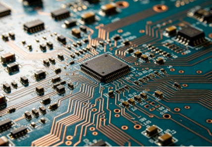
PCB assembly choices strongly impact product dependability, expense management, and lasting steadiness in B2B electronics making. In actual factory settings, picking among SMT, wave soldering, and reflow soldering is not merely a technical matter. It is also a hazard management choice. This choice affects success rates and delivery steadiness. At PCBA Store, we offer organized PCB Assembly services. We assist engineering groups to pair process choices with actual product needs and output size.
This post looks at the real differences among these joining techniques. It also shows how to pick the proper soldering PCB process for commercial uses.
SMT vs SMD in PCB Manufacturing Structure
SMT vs SMD is a frequent mix-up in PCB buying and engineering talks. Still, the two words detail distinct levels of the identical framework.
SMT (Surface Mount Technology) points to the PCB assembly routine. Here, parts are put straight onto the board face. SMD (Surface Mount Device) points to the electronic items crafted for SMT assembly.
This contrast counts in BOM layout and making plans. This is because SMT sets the process sequence, while SMD sets part matching.
Item | Meaning | Function in PCB Assembly |
SMT | Assembly process | Surface mounting technology |
SMD | Component type | Parts used in SMT process |
SMT is broadly applied in highly packed PCB layouts. It aids automation. It cuts down on hole-making. It boosts output speed. It acts as the base of current PCB making for small electronic setups.
Wave Soldering Process in PCB Assembly
Wave soldering is an older PCB joining method. It is mostly applied to through-hole parts and mixed-tech boards.
During this step, the PCB moves over a fluid solder wave. This lets solder link with bare metal pins. It is frequently applied in power electronics. It is also used in factory control setups and big connector builds.
Wave soldering gives firm physical links. This makes it fit for spots with shaking, heavy current, or physical strain.
Yet, it does not fit highly packed SMT layouts. This is due to solder bridging hazards and poor exactness control. Heat contact is also greater when matched against SMT reflow steps.
From a making hazard view, wave soldering is picked when physical firmness matters more than making things tiny.
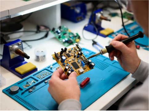
Reflow Soldering in SMT-Based PCB Assembly
Reflow soldering acts as the main step applied in SMT output lines. It is also key in current PCB Assembly setups.
The step involves solder paste laying, part setting, and steady warming inside a reflow oven. The solder turns liquid. It then builds exact electrical links during the cooling phase.
Reflow soldering fits highly packed electronics. These need exactness and steady results. It fully matches automated output setups. This drops worker mistakes and boosts steadiness.
Main control spots include heat curve exactness and warming evenness. Bad control can spark flaws. These include solder gaps, tombstoning, or weak links.
In current PCB making, reflow soldering is the standard step for SMT-based layouts. This is due to its growth ease and exactness.
Wave Soldering vs Reflow Soldering: Key Differences
The match-up of wave soldering vs reflow soldering points out two totally distinct building paths.
Wave soldering is tuned for through-hole firmness. Meanwhile, reflow soldering is crafted for SMT exactness and packing.
Parameter | Wave Soldering | Reflow Soldering |
Component type | Through-hole | SMD |
Precision level | Medium | High |
Automation level | Medium | High |
Mechanical strength | High | Medium |
Best application | Power boards | Dense PCB layouts |
Reflow soldering aids current shrinking shifts. On the other hand, wave soldering stays vital for physical toughness and heavy-duty uses.
In numerous factory projects, both steps are applied hand in hand within mixed PCB Assembly layouts.
Soldering PCB Process Selection Logic
Picking the proper soldering PCB process relies on the item build. It also rests on working needs and output size.
Highly packed talk boards lean mostly on SMT and reflow soldering. This is due to room limits and signal purity needs. Factory power setups often apply wave soldering. This grants firmer physical links.
The picking logic usually rests on three main points:
l PCB component mix (SMT vs through-hole ratio)
l Mechanical stress and operating environment
l Production volume and cost efficiency
Wrong process picking can push up flaw rates and long-term fix hazards. This is very true in mass output settings.

Hybrid PCB Assembly for Industrial Applications
Mixed PCB Assembly merges SMT reflow soldering and wave soldering into one output path.
In this build, SMT parts are put together first. This uses reflow soldering. Through-hole parts are then handled using wave soldering.
This path is broadly applied in factory-grade electronics. These need both high wire packing and firm physical steadiness.
Main perks include:
l Improved structural strength for vibration environments
l Flexibility in component selection
l Balanced cost and performance control
Mixed building needs exact process ordering. This stops heat harm and solder clashing.
Quality Control and Risk Management in PCB Assembly
PCB pureness rests on strict checking across every output phase. Even tiny process shifts can hurt long-term dependability in mass output.
Main checking steps include:
l Incoming material verification
l AOI optical inspection during SMT production
l Functional testing based on application requirements
l Final assembly inspection before shipment
Heat control during reflow and wave soldering is vital. It stops solder link weariness and unseen flaws. Tracking setups ensure steady purity across output groups.
Application Scenarios for Different Soldering Methods
Distinct joining ways are picked based on use needs and dependability hopes.
SMT and reflow soldering are broadly applied in:
l Communication equipment
l Consumer electronics
l High-density control boards
Wave soldering is frequently applied in:
l Power supply systems
l Industrial automation equipment
l Heavy-duty connector assemblies
Mixed PCB Assembly is put to use in setups needing both packing and toughness. Examples include energy setups and transit electronics.
PCBA Store Manufacturing Capability and Process Control
At PCBA Store, we offer PCB Assembly services. These are crafted for global B2B engineering groups. They need steady output and strict hazard management.
Our output setup supports SMT lines and wave soldering lines. It also runs mixed building paths under set making states.
Engineering help and pricing are open via PCBA Store web setup. There, users can load Gerber files and BOM lists for quick checking.
Our main skills include:
l SMT assembly for high-density PCB designs
l Wave soldering for through-hole and power components
l Mixed-process PCBA integration for industrial applications
l DFM analysis to reduce production risk before scaling
We center on process steadiness and flaw blocking. This backs long-term bond making.
Conclusion: Selecting the Right PCB Soldering Strategy
SMT, wave soldering, and reflow soldering each fill distinct spots in PCB making. The proper soldering PCB process directly impacts product dependability. It also shapes expense budgets and output stability.
At PCBA Store, we back B2B buyers with organized PCB Assembly plans. These are crafted for large output and strict making hazard control. Engineering groups can load project files. This grants quick technical checking and pricing.
FAQ: PCB Assembly Process and Manufacturing Decisions
How is PCB Assembly pricing calculated in SMT and wave soldering projects?
Pricing relies on part packing, process kind, and PCB layers. It also rests on testing needs and output size. SMT-heavy layouts mostly need greater building and checking work.
What is the main difference between wave soldering and reflow soldering?
Wave soldering is applied to through-hole parts needing greater physical firmness. Meanwhile, reflow soldering is applied for SMT parts needing exactness and packing.
Can SMT and wave soldering be combined in one PCB Assembly project?
Yes. Mixed PCB Assembly is broadly applied in factory electronics. It merges SMT exactness with through-hole toughness.
What quality control methods are used in PCB manufacturing?
Frequent ways include AOI checking and working tests. They also involve item tracking and process watching during joining phases.
How can production risks be reduced in PCB Assembly?
Hazards can drop through proper process picking. DFM checking before output and early model testing also helps.



