General, quoting & support.
Add: Building E, No.58, Nanchang Road, Xixiang , Baoan District Shenzhen City, Guangdong, China
Tel : 0755-27348887
Fax : 0755-27349876
E-mail : svc@pcbastore.com

PCB Thermal Management Guide for Reliable Boards
PCBA Store / 2026-09-02
Contents [hide]
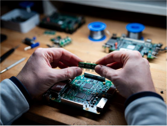
Heat issues seldom show up as just one hot part. Instead, they cause shaky performance. They also lead to shorter part lifespans and solder fatigue. Customers might return products. You could avoid these failures. You just need to plan the board stack-up, copper layout, and cooling routes together.
Heat Flow Defines the Whole Board Decision
A solid cooling strategy starts with the heat's path. Warmth must travel from the component junction to the outside air or casing. High-current power stages and LED drivers generate local heat. Motor controls, AI edge modules, and small industrial controllers do this too. This warmth has to move through copper, dielectric layers, vias, and outer metal parts. Finally, it can leave the assembly.
Design teams must view thermal management as both an electrical and mechanical task. They need to do this at the same time. Trace width and copper weight matter. Component density, airflow, and enclosure contact are also important. Furthermore, assembly process limits play a big role. All these factors decide if a factory can build the design reliably.
PCB Materials Shape Thermal Resistance
Choosing the right substance dictates how fast heat escapes a source. It also affects how well the circuit board survives constant temperature changes. Standard FR-4 is still popular for basic control electronics. However, higher thermal needs might demand different choices. You might need high-Tg FR-4 or an aluminum base. Ceramic-filled options, PTFE, or other specific laminates could also be necessary.
PCBA Store supports FR-4, polyimide, aluminum, ceramic, PTFE, Rogers, and related material options, so overseas buyers can align the stack-up with the application instead of treating the board as a commodity item. For a design that runs warm, the most useful early question is whether the selected PCB materials still match the heat path, current load, and assembly process.
Design choice | Thermal role | Typical use case |
High-Tg FR-4 | Improves stability under higher operating temperature | Industrial controls and dense multilayer boards |
Aluminum substrate | Moves heat toward a metal base | LED modules and power boards |
Heavy copper | Spreads current and heat through thicker conductors | Power conversion and motor control |
Thermal vias | Transfers heat between layers or toward a heat sink | BGAs, QFNs, regulators, and compact modules |
Copper Planning Controls Hot Spots
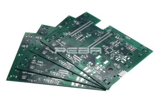
You must plan copper weight and copper shapes at the same time. A well-planned heavy copper PCB can handle more electrical current. It also spreads warmth better than a standard circuit board. However, thick copper alone cannot fix a narrow trace neck. It will not solve a weak plane link or tightly packed components.
Wide lines, solid planes, and balanced copper zones are crucial. Short thermal routes usually matter more than a single high copper thickness number. PCBA Store offers rigid board production up to 30 oz sample copper. They also support 6 oz mass copper. This makes the design review phase very important. Line width, spacing, drill limits, and surface finish choices must stay easy to manufacture.
Trace and plane geometry
Trace shapes must stop blockages near connectors and MOSFETs. Inductors, LEDs, and power regulators need clear paths too. When electricity flows through a narrow metal line, resistance goes up in that specific spot. This turns that small area into a heater. This happens even if the rest of the board features plenty of copper.
Thermal via patterns
Thermal vias must link the heat source to actual copper areas. These areas need to spread or release the warmth effectively. Via-in-pad designs, filled holes, and via groups can assist small products. Still, you should match them to your soldering, inspection, and budget goals. Do not just copy them from a basic layout guide.
Layout Guidelines Need Manufacturing Reality
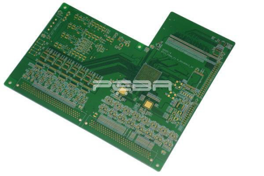
Good layout rules reduce risk only when they match the fabricator's real process window. Minimum trace and spacing, drill diameter, aspect ratio, solder mask clearance, surface finish, and impedance tolerance can all constrain a thermal design.
A practical review uses manufacturable PCB design guidelines as a manufacturing filter, not as a separate checklist after the layout is finished. High-power boards should be checked for copper balance, panel behavior, thermal expansion, solder joint access, and inspection visibility before the first build.
· Place heat-generating parts where airflow, copper area, and mechanical contact can support them.
· Avoid narrow copper necks between a hot component and its heat-spreading plane.
· Keep thermal vias useful by connecting them to meaningful copper or metal surfaces.
· Review solder mask openings and finish choice around high-current pads early.
Assembly and Testing Close the Thermal Loop
Thermal design continues through PCB assembly because solder volume, stencil design, reflow profile, component package, and inspection method all influence real heat transfer. BGAs, QFNs, large thermal pads, and bottom-terminated components may need X-ray inspection or special stencil treatment to confirm that the intended path is physically present.
The cooling plan should also account for what happens after shipment. Enclosures, mounting screws, conformal coating, nearby heat sources, dust, airflow restriction, and operating duty cycle can change board temperature after laboratory testing, so acceptance criteria should reflect the real installation.
PCBA Store offers SMT, through-hole, mixed assembly, lead-free and leaded options, X-ray inspection, AOI, ICT, and functional testing. These capabilities help teams verify not only whether the circuit turns on, but whether the assembled board can support the intended operating load.
Summary for Thermal Design Decisions
A reliable thermal PCB is created by matching material, copper, vias, layout, assembly, and cooling hardware to the same heat-flow goal. Buyers should confirm the heat source, operating environment, acceptable temperature rise, board technology, and inspection needs before freezing the design.
For industrial, medical, robotics, drone, or AI electronics that need a manufacturable thermal path, PCBA Store can review PCB fabrication and PCB assembly requirements against the actual application before production.
FAQ
What is PCB thermal management?
PCB thermal management is the design of materials, copper, vias, component placement, and cooling paths so heat moves away from sensitive or high-power components safely.
When should a design use heavy copper?
Heavy copper is useful when current, heat spreading, or mechanical durability exceeds what standard copper can handle, but it must be reviewed for manufacturability.
Do thermal vias always improve cooling?
Thermal vias help when they connect the source to an effective plane, heat sink, or metal area. Poorly placed vias can add cost without solving the main heat path.
Which PCB board material is best for heat?
The best PCB board material depends on temperature, power density, signal needs, cost, and mechanical design. FR-4 may work, while metal-core or ceramic options may suit hotter products.
Why involve the assembly supplier early?
The assembly supplier can check stencil design, reflow limits, inspection access, component packages, and test planning before thermal assumptions become expensive production problems.
Previous article:How Overseas Buyers Source PCB Assembly Services



