General, quoting & support.
Add: Building E, No.58, Nanchang Road, Xixiang , Baoan District Shenzhen City, Guangdong, China
Tel : 0755-27348887
Fax : 0755-27349876
E-mail : svc@pcbastore.com

SMT Assembly Challenges and Engineering Fixes
PCBA Store / 2026-09-04
Contents [hide]
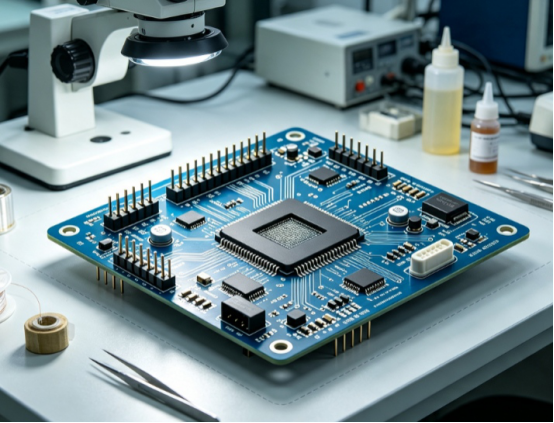
SMT defects often look small under magnification but large in business impact. A bridge, tombstone, shifted component, or hidden BGA void can delay a launch, consume engineering time, and turn an otherwise sound PCB design into an unreliable product.
Defects Usually Begin Before Reflow
Most SMT assembly problems start with the relationship between land pattern, solder paste volume, component geometry, board finish, and placement accuracy. Reflow exposes the weakness, but the root cause is often already present during printing or placement.
For industrial, medical, robotics, drone, and AI electronics, the cost of rework is more than a repair expense. Each defect can affect calibration, signal stability, thermal behavior, or final product confidence, so prevention matters more than fast troubleshooting.
The strongest engineering response is to connect every defect with a controllable input. Paste height, pad geometry, storage condition, placement pressure, reflow profile, and inspection threshold should be measured as process variables, not treated as isolated production complaints.
Solder Paste Printing Sets the Process Window
Paste printing is the first high-risk stage because it controls solder volume on every pad. Too much paste can create bridges or solder balls, while too little paste can create opens, weak fillets, or intermittent joints after vibration and thermal cycling.
A stable controlled SMT assembly process uses stencil thickness, aperture shape, paste type, board support, and printer setup as one system. PCBA Store uses auto solder-paste printing with SPI, which supports early detection before defects move deeper into production.
Challenge | Likely cause | Engineering control |
Solder bridge | Excess paste, tight pitch, poor mask clearance | Stencil aperture tuning and paste inspection |
Tombstoning | Uneven wetting or thermal imbalance | Balanced pad design and reflow profiling |
Component shift | Placement force, paste slump, board movement | Stable support and placement verification |
BGA voids | Poor escape path or reflow profile | Pad design review and X-ray inspection |
Placement Accuracy Depends on Data Quality
Placement is only as reliable as the data used by the machine and the fixtures supporting the board. Centroid data, polarity marks, component rotation, package naming, and panel fiducials should be checked before production starts.
PCBA Store's process requires PCB files, BOM, centroid data, and other necessary documents before assembly timing begins. This requirement helps prevent the common situation where a board enters production with unresolved orientation or package mismatches.
Component package variation
Package variation becomes serious when alternate manufacturer part numbers are treated as exact substitutes. A small pad, height, polarity, or moisture-sensitivity difference can change soldering behavior even when the electrical value looks correct.
Component data should therefore identify approved manufacturers, package codes, polarity conventions, and any parts that require buyer approval before substitution. That record protects the electrical design while giving sourcing teams enough flexibility to avoid unnecessary delays.
Panel support and fiducials
Panel support keeps thin or routed boards flat during printing and placement. Good fiducials let the placement system correct board position, which is especially important for fine-pitch ICs and small passive packages.

Reflow Quality Needs Profile Discipline
Reflow is where paste, board finish, copper balance, and component mass meet one thermal curve. A profile that works for one board can fail another if the assembly has large copper planes, mixed package sizes, or sensitive components.
A mature repeatable SMT process control plan controls soak, peak temperature, time above liquidus, and cooling rate without treating the oven as a black box. Thermal profiling helps keep solder joints consistent while protecting components and laminate integrity.
Mixed-technology boards need extra care because through-hole mass, connectors, shields, and heat sinks can pull heat away from nearby SMT joints. The reflow profile should protect small passives while still giving larger packages enough energy for proper wetting.
· Confirm moisture-sensitive components before reflow exposure.
· Use SPI and AOI results to catch process drift early.
· Review BGA, QFN, and fine-pitch areas with inspection methods that can see hidden joints.
· Tie functional testing to the customer's real use case, not only power-on behavior.
Inspection Turns Defects into Process Feedback
Inspection is most useful when results feed back into process settings. AOI can catch visible defects such as missing parts, polarity errors, paste issues, and solder bridges, while X-ray is important for hidden terminations under BGA and QFN packages.
PCBA Store combines visual inspection, AOI, ICT, X-ray inspection, and functional testing for PCB assembly work. A complete SMT PCB assembly plan should connect these checks to the defect risks of the actual board, not simply run the same inspection list for every design.
Inspection data should be discussed with the engineering team when a pattern repeats. A repeated bridge, skew, insufficient solder joint, or voiding issue is rarely solved by one repair; it usually points to stencil, placement, profile, component, or land-pattern correction.
Summary for Better SMT Yield
SMT yield improves when teams control paste, placement data, reflow, inspection, and feedback together. The practical next step is to review land patterns, BOM substitutions, centroid files, panel design, and test expectations before production rather than after defects appear.
PCBA Store can support prototype and production PCB assembly with SMT, THT, mixed technology, turnkey or kitted parts, and inspection planning for demanding electronic products.
FAQ
What are the most common SMT assembly defects?
Common defects include solder bridges, tombstoning, open joints, shifted parts, missing components, wrong polarity, insufficient solder, voiding, and hidden BGA connection problems.
Why does tombstoning happen in surface mount technology?
Tombstoning usually happens when wetting force is uneven between two pads because of layout imbalance, paste variation, placement offset, or uneven heating during reflow.
How does SPI help an SMT line?
SPI checks solder paste volume and shape before components are placed, so the team can correct printing issues before they become reflow defects.
When is X-ray inspection needed?
X-ray inspection is useful for BGAs, QFNs, CSPs, and other packages where solder joints are hidden under the component and cannot be judged by surface inspection.
Can a prototype SMT process scale to production?
A prototype process can scale when the design, BOM, panel, stencil, profile, and inspection data are documented clearly enough to repeat at higher volume.
Previous article:Rigid-Flex PCB Applications in Compact Electronics



