General, quoting & support.
Add: Building E, No.58, Nanchang Road, Xixiang , Baoan District Shenzhen City, Guangdong, China
Tel : 0755-27348887
Fax : 0755-27349876
E-mail : svc@pcbastore.com

Top PCB Assembly Defects and How to Prevent Them During Production
PCBA Store / 2026-08-21
Contents [hide]
Assembly defects rarely begin at the final inspection station. They usually develop when design data, materials, printing, placement, soldering, handling, and test requirements do not form one controlled production path. For engineers and procurement teams, prevention means defining the process window before the first board runs, then using inspection data to correct drift before it becomes a shipment problem.
Why Defects Cluster at Process Handoffs
A PCB passes through several ownership changes: design releases files, purchasing sources parts, production prepares materials, machines place components, ovens form joints, and inspectors judge the result. A small ambiguity at one handoff can multiply. An incorrect polarity note becomes repeated placement; an unapproved alternate changes wetting; or an incomplete panel drawing causes board support problems during printing.
Paste and placement errors begin before reflow
Paste volume must match each soldering pad, stencil design, paste condition, and printing parameters. Too little paste can leave open or weak solder joints, while excess or smeared paste can encourage bridges and solder balls. Placement adds another variable: offset parts, reversed polarity, wrong values, or disturbed deposits may survive until the board enters the oven. Solder-paste inspection and first-article verification catch these errors while correction is still inexpensive.
Thermal and mechanical variation reshape the joint
A cold solder joint can result when surfaces do not wet correctly or the joint experiences unsuitable heat or movement. Large copper areas, shields, connectors, and small passives heat at different rates, so one generic oven setting may not suit the loaded board. A measured profile should stay inside paste and component limits while giving demanding joints enough time to form correctly.
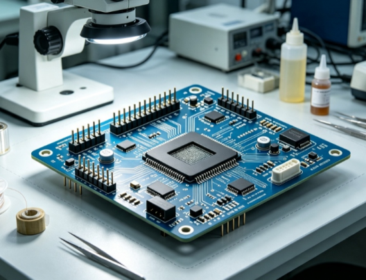
Common Defects and the Controls That Stop Them
Defect | Typical process signal | Preventive control |
Open or weak joint | Low paste, poor wetting, movement | Stencil review, material control, measured profile |
Solder bridge | Excess paste or placement offset | Aperture tuning, printer setup, SPI |
Tombstoning | Unequal wetting or thermal balance | Symmetric pads, balanced heating |
Insufficient solder | Low deposit or blocked aperture | Stencil cleaning and deposit measurement |
Hidden-joint anomaly | Paste, outgassing, thermal profile | Process trials and X-ray where justified |
Wrong or reversed part | BOM, feeder, or polarity error | Approved BOM, setup verification, AOI |
This table is a diagnostic starting point, not a universal root-cause verdict. Similar-looking solder joints can have different causes, and one soldering pad may combine design, material, and process factors. The response should preserve the affected sample, review process records, compare good and failed locations, and verify the suspected cause through a controlled correction.
Prevent Defects Before the Line Starts
Release complete and unambiguous build data
Production should receive released Gerber files, an approved BOM, centroid or pick-and-place data, assembly drawings, polarity references, approved alternates, solder requirements, and test instructions. Revision identifiers must agree across the package. Clear data protects the line from informal interpretation and gives inspectors a defined reference when a component or drawing appears inconsistent.
A disciplined PCB assembly process reviews manufacturability before materials are committed. Fiducials, panel rails, component-to-edge spacing, thermal-pad apertures, test access, and package orientation all affect SMT assembly stability. PCBA Store supports SMT assembly, through-hole, mixed-technology, and single- or double-sided placement, so the route should follow the actual board rather than its component count.
Control materials and the thermal window
Moisture-sensitive devices, solder paste, bare boards, and component finishes require controlled storage and handling. Paste condition and working time affect print repeatability; exposed components may need documented floor-life management; and contaminated surfaces can resist wetting. The oven profile then needs measurement on a representative assembly, including both fast-heating and slow-heating locations.
· Approve substitutions before loading feeders, not after inspection finds a mismatch.
· Verify stencil revision, support tooling, paste condition, and printer setup at changeover.
· Check the first article for value, polarity, orientation, alignment, and joint formation.
· Track recurring defect locations by board, package, machine, shift, and lot.

Use Inspection as Process Feedback
Inspection methods answer different questions. Visual inspection finds obvious workmanship or handling problems. AOI supports repeated checks for placement, polarity, and visible joint conditions. X-ray is useful for concealed interconnections such as BGA and QFN packages. ICT can isolate electrical faults when access exists, while functional testing evaluates behavior against a defined procedure. None of these methods automatically replaces the others.
Effective PCBA testing connects each failure to disposition and corrective action. PCBA Store lists visual inspection, AOI, X-ray, ICT, and functional testing among its available PCBA testing methods. Buyers should specify which tests apply, acceptance criteria, required records, fixture ownership, and how a failed unit is analyzed instead of merely asking for full testing.
IPC-A-610 is widely used to communicate electronic-assembly acceptance criteria, while IPC J-STD-001 addresses process and material requirements for soldered assemblies. The purchase order should identify the required revision, class, customer exceptions, and supporting records. A standard name on a supplier page does not prove that every quoted build follows the buyer's intended acceptance plan.
Summary: Make Prevention Measurable
The most reliable way to reduce PCB assembly defects is to control inputs, confirm the first article, measure printing and thermal windows, and treat PCBA testing results as production feedback. Buyers should judge a supplier by how clearly it links a defect or damaged soldering pad to data, containment, root cause, and verified correction, not by a promise that defects never occur.
For a production review, send PCBA Store your build package with released files, quantity, solder requirements, inspection scope, test procedure, and acceptance criteria.
FAQ
What are the most common PCB assembly defects?
Common findings include opens, weak joints, bridges, solder balls, tombstoning, insufficient solder, wrong or reversed components, hidden-joint voids, and damage caused by uncontrolled rework or handling.
How can solder bridges be prevented?
Review stencil apertures and pad geometry, control paste condition and printer setup, verify placement accuracy, keep the stencil clean, and detect excess deposits before reflow.
Does AOI detect every soldering defect?
No. AOI is strong for visible features, but concealed joints may require X-ray, and electrical or functional faults may require ICT or functional testing.
Why is a board-specific reflow profile necessary?
The loaded board contains different thermal masses. Measurement shows whether small and large joints remain within paste and component limits without underheating one area or overheating another.
What should a buyer provide before SMT assembly begins?
Provide synchronized Gerber, BOM, centroid, and drawing revisions; approved alternates; polarity references; solder requirements; quantities; inspection criteria; test procedures; and any programming, coating, or packing instructions.
Previous article:PCB Repair or Replacement - How to Decide the Best Solution



