General, quoting & support.
Add: Building E, No.58, Nanchang Road, Xixiang , Baoan District Shenzhen City, Guangdong, China
Tel : 0755-27348887
Fax : 0755-27349876
E-mail : svc@pcbastore.com
Everything About Via in Pad Technology
Simon / 2021-02-13
Contents [hide]
Via in Pad is one of the most impressive technologies to ever be discovered, and its influence has transformed the digital world. Unfortunately, their application is rather complicated than expected. It is employed in electronic products and fine pitch devices to help offer interconnection benefits between PCB layers. Via in Pad has also fostered the miniaturization of SMD chips and necessitated the development of high-density BGAs. This has enabled Via filling without using chemicals, hence keeping soldering errors at bay. The technology has also enabled extra conductor BGA traces, making it a safe and reliable option in the production process. Before digging deeper into Via in Pad, let's comprehend what the whole technology entails.

What is a Via in Pad technology?
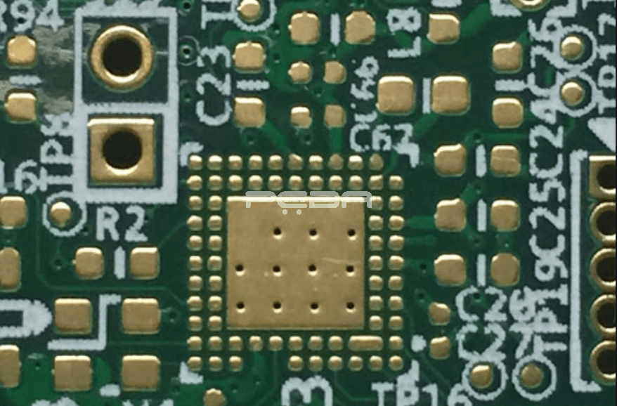
When considering technology in PCB fabrication or PCB design, Via in Pad entails a PCB design to boost PCB density. This enables higher component density, especially in BGA and SMT areas. It can also be defined as the Pad having plated holes that link copper tracks layer to another. High-density PCB multi-layer can include blind vias, which can only be seen on one surface. It can also have buried vias, which can be seen on neither, a concept known as micro vias. The broad and advent utilization of small pitch devices and the need for finer size PCBs causes a new issue. The only solution to these issues is using the current PCB technology "via in pad'.
The use of via in pad technology helps minimize inductance and boost the density while using finer or smaller pitch package. The strategy employed here introduces directly via under the contact pad of the device. This approach gives room for higher density components and boosts the routing process. However, the technology offers the designers excellent PCB space savings. For instance, traditional devices fan-out introduces four components. With via in Pad, the board uses up to six components. If you are looking forward to getting intermediate density, you can consider filled via in Pad. It has an intermediate cost, unlike using buried or blind vias. Some primary benefits linked with this technology are explained below.
Advantages of Via in Pad
There are many compelling reasons to consider using via in pad technology for PCB design. Firstly, it is appropriate for boosting the PCB density; it also reduces the inductance and still uses a more solid pitch package. Since the via is placed directly under the contact pad device, it is easy to achieve great part density and overwhelming routing. Compared to buried vias and blind vias, other reasons to consider using via in Pad are:
More essential for fine pitch PCB and BGA
Great performance in heat dissipation and thermal management
Minimize inductance in PCB board (high-frequency)
Work wonders in boosting the PCBs density and save an excellent PCB space
Secures a flat area for the SMD components
Handle high-speed PCB limits
Leads to more routing and sizeable PCB package
Due to these overwhelming reasons, via in Pad are broadly employed for finer PCBs, particularly for high-end designs and the BGAs that demand little space. Although other options such as buried vias and blind vias have beneficial characteristics for boosting the density and saving space for PCBs, via in pads are exceptional when it comes to high-end design elements and thermal management. Furthermore, via in Pad can be placed into the QFN package components and SMT pads.
Different types of Vias
Based on the functionality or feature, various kinds of vias are connected to a PCB. They include:
1. Buried via
This option links the internal board layer and is essential for PCBs that require high routing.
2. Thru-hole via
This via is a kind that is employed mostly in standard circuit PCBs. Basically, the holes are made on the board using a mechanical drill bit. The size can go up to 6 mils.
3. Blind via
This via option can start on the bottom or the top of the PCB; however, the hole doesn't penetrate through it.
4. Microvia
Where smaller holes less than 6 mils are required, the microvia option is the most preferred. Microvia links adjacent board layers and can be buried on the board's layer or on the surface of the board. This option is highly versatile, which means it can be stacked on top of the buried via or stacked together. They are also believed to have a more significant PCB fabrication cost.
5. Via in pad
This is a special type of via that can be used as standard microvias or thru-hole vias. They are also exceptionally positioned on the mount pad surface, making them unique. When using a standard mechanical drill, via in pad demands an additional fabrication process to stop solder from flowing into the hole. Microvias option, however, doesn't portray such issues, but it is challenging to fabricate because of its space tolerance and tighter trace in high-end design.
With these options, the kind of via to employ basically depends on the PCB technology, cost of the fabrication, and the circuitry requirements. For example, a microvia option is desirable to consider using due to its smaller size; however, that capability doesn't make it the right option. A microvia technically has several steps during fabrication; hence more expensive. For a high-end interconnect board, considering microvia is the right choice.
When should I use Via in pad
If you try routing and avoid a package of components containing 0.5mm sub pitch using traditional ways of routing, it will result to check errors because of an annular ring, trace width, and the limitation of the drill size. Manufacturing issues on the trace size doesn't employ compact and smaller traces to be created using PCB traditional fabrication ways. Therefore, for components with a small pitch, the solo and workable method to route them is considered capped via in pad because it enables routing of the PCB to be highly compact.
Capped via in pad also makes complicated LGA and BGA packages to be as simple as possible. Rather than considering traditional fan-out, via in pad produces signals that travel directly into the PCB. Routing on the surface is reduced, enabling components such as bypass capacitors and the rest to be closely placed, reducing parasitic inductance. Additionally, this allows short ways to ground and power planes, which helps reduce EMF.
In thermal pads, via also assist in heat management. Typically, high power mount part surface possess a thermal pad that is designed to mount on to the PCB. To efficiently dissipate more heat, it is recommended to drop vias from the PCB to the other PCB side. So should you use via in every pad? Well, the benefit earned in minimizing the fan out components and routing challenges is offset by enhancing material cost and manufacturing complications of the PCB fabrication process. In case the design of the hardware component can be achieved using the traditional via routing method, then it is good to avoid using via in pad.
Via in pad guidelines for PCB
Via in pad for PCB entails a complicated procedure. Fortunately, it can be easy if you consider learning the ropes from the experts. What happens is that via must be plugged by resin and placed flat using copper. It is also be applied in small BGA. The process basically fills the via hole using a non-conductive or conductive material. What follows is plating via over, offering a smooth and flat surface that can be soldered.
Via in the pad are applied in PCB designs that allow components to be mounted over. It is also useful in the solder joint that helps extend it over the via. There is a myth that a non-conductive material fill can pass little to no electrical signal through such via. The idea is that these are just misconceptions. The vias barrels will equally be plated with material like copper as it would have been with others via materials on the board. The sole thing that makes a difference between them is the empty air in the barrel that is mostly replaced using full materials. Doing this helps to stop contaminants such as solder from getting into the via or offer a structural backbone for the copper pad holding the open hole in the via.
Processing capability
Minimum pad capacity for VIA: Drill plus 0.15mm
Minimum drilling capacity: 0.20mm
Conclusion
The increase in electronic components has undoubtedly led to discovering other new technology and tools to use in such components in a scalable and reliable manner. Via in pad enables fan-out, which is the smallest component with PCB design techniques. If you are looking forward to utilizing via in pad technology, you will need to ponder additional manufacturing cost and the time required. For the best results, consider working with professional PCB manufacturers to learn the ropes and guide you on making better decisions. Working with manufacturer makes you an expert in the field, which means you can guide others looking forward to learning the same.
Previous article:What is PCB Tenting Vias?


