General, quoting & support.
Add: Building E, No.58, Nanchang Road, Xixiang , Baoan District Shenzhen City, Guangdong, China
Tel : 0755-27348887
Fax : 0755-27349876
E-mail : svc@pcbastore.com

What are the steps of assembly PCB board ?
Emma / 2018-01-09
Contents [hide]
As you know , i do not only make PCB board , but also assembly the parts on PCB board . Then what are the steps of assembly PCB board ?
1. make stencil and apply for solder paste

The first step of PCB assembly is applying a solder paste to the board. This process is like screen-printing a shirt, except instead of a mask, a thin, stainless-steel stencil is placed over the PCB. This allows assemblers to apply solder paste only to certain parts of the would-be PCB. These parts are where components will sit in the finished PCB.
In a professional PCB assembly line, a mechanical fixture holds the PCB and solder stencil in place. A brusher then places solder paste on the intended areas in precise amounts. The machine then spreads the paste across the stencil, brush it evenly to every open area. After removing the stencil, the solder paste remains in the intended locations.
2. Pick and Place
After brushing the solder paste to the PCB board, the assembly process moves on to the pick and place machine ( PCBA STORE SMT machine : Yamaha , Panosonic )
Traditionally, this was a manual process done with a pair of tweezers, in which assemblers had to pick and place components by hand. These days, thankfully, this step is an automated process among PCB manufacturers. This shift occurred largely because machines tend to be more accurate and more consistent than humans. While humans can work quickly, fatigue and eyestrain tends to set in after a few hours working with such small components. Machines work around the clock without such fatigue.The device starts the pick and place process by picking up a PCB board with a vacuum grip and moving it to the pick and place station. The robot then orients the PCB at the station and begins applying the SMTs to the PCB surface. These components are placed on top of the soldering paste in preprogrammed locations.This called SMT

3: Reflow Soldering
Once the solder paste and surface mount components are all in place, they need to remain there. This means the solder paste needs to solidify, adhering components to the board. PCB assembly accomplishes this through a process called "reflow. "
After the pick and place process concludes, the PCB board is transferred to a conveyor belt. This conveyor belt moves through a large reflow oven, which is somewhat like a commercial pizza oven. This oven consists of a series of heaters which gradually heat the board to temperatures around 250 degrees Celsius, or 480 degrees Fahrenheit. This is hot enough to melt the solder in the solder paste.
Once the solder melts, the PCB continues to move through the oven. It passes through a series of cooler heaters, which allows the melted solder to cool and solidify in a controlled manner. This creates a permanent solder joint to connect the SMDs to the PCB

4.Inspection and Quality Control
Once the surface mount components are soldered in place after the reflow process, the board can be tested for functionality. Often, movement during the reflow process will result in poor connection quality or a complete lack of a connection. Shorts are also a common side effect of this movement, as misplaced components can sometimes connect portions of the circuit that should not connect.
And the most common of these inspection methods include the following:
Manual Checks
Automatic Optical Inspection ( called AOI )
X-ray Inspection ( used most often for more complex or layered PCBs. )

5.Through-Hole Component Insertion ( THT ) - normally by hand
Depending on the type of board under assembly, the board may include a variety of components beyond the usual SMDs. These include plated through-hole components, or PTH components.
After this soldering process is finished, the PCB can move on to the final inspection, or it can run through the previous steps if the PCB needs additional parts added or another side assembled.
 - normally by hand")
6. Final Inspection and Functional Test
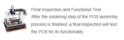
After the soldering step of the PCB assembly process is finished, a final inspection will test the PCB for its functionality. But you have to offer us test way . ( Also if you want to burn IC programming , you have to offer the programming and burn way to assembler like us ) . Sometimes , some people would sue test fixture , ( text jig ) , you would send me the requirement and details of test jig .
After all of these , then you assembly job finish .
Want to know more ?
Emma Mai would tell you everything she knows .
Previous article:How to solder onto PCB


