General, quoting & support.
Add: Building E, No.58, Nanchang Road, Xixiang , Baoan District Shenzhen City, Guangdong, China
Tel : 0755-27348887
Fax : 0755-27349876
E-mail : svc@pcbastore.com

What Is PCB Stencil and How It Improves SMT Accuracy
PCBA Store / 2026-07-24
Contents [hide]

Introduction
Today, electronic devices require smaller elements, higher density of circuits, and consistency in manufacturing. In the process of SMT PCB assembly, one of the most important steps is printing the solder paste. The design of the PCB stencil plays an essential role in achieving high-quality solder joints.
What Is a PCB Stencil and What Is Its Purpose in SMT Assembly?
PCB stencil is a specially made metal plate. The main function of this device is to deposit solder paste on the pads of the printed circuit board before mounting components. In the course of SMT, the stencil gets aligned to the surface of the PCB, and then the solder paste goes through the specially made holes.
In other words, the use of the stencil helps to manage the position of the solder paste as well as the amount of solder paste applied. Modern PCBs typically have fine-pitch components and dense packing.
The SMT printing process includes several main steps:
Process Step | Purpose |
PCB alignment | Matches stencil openings with PCB pads |
Solder paste printing | Applies accurate solder paste deposits |
Component placement | Positions electronic components |
Reflow soldering | Creates permanent solder connections |
Inspection | Checks assembly quality |
At PCBA Store, we combine PCB stencil requirements with the full PCB manufacturing and assembly workflow. Our engineers review PCB design, component packages, and production needs. This supports reliable SMT PCB Assembly.
Why Is PCB Stencil Important for SMT PCB Assembly?
A PCB stencil directly affects solder paste quality. This quality touches every later SMT process. The right stencil design makes sure each pad gets the correct amount of solder paste before component placement.
Controlling Solder Paste Volume
Solder paste volume needs accurate control. Too much paste or too little can create assembly issues.
Excess solder paste may cause bridging between close pads. This risk rises with fine-pitch components. Too little solder paste can produce weak joints, open circuits, and low mechanical strength.
PCB Stencil Factor | Impact on Assembly |
Thickness | Controls solder paste volume |
Aperture size | Determines paste amount |
Aperture design | Improves paste release |
Alignment accuracy | Prevents printing offset |
A proper stencil thickness and aperture design help manufacturers reach consistent solder deposits on varied PCB layouts.
Supporting Miniaturized Components
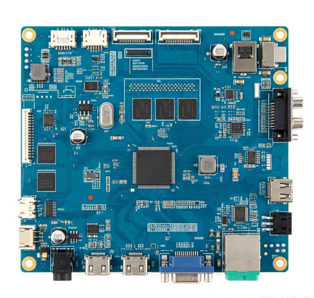
Modern electronics use smaller parts such as 0201, 01005, QFN, and fine-pitch IC packages. These parts demand accurate solder paste printing. The soldering area stays limited.
A high-quality PCB stencil improves paste position. It gives a stable base for automated pick-and-place machines. This cuts problems such as component movement and tombstoning during reflow soldering.
How Does PCB Stencil Reduce SMT Defects?
Stencil design shares a direct link with common SMT manufacturing defects. Better stencil parameters help lower rework and raise final PCBA reliability.
SMT Defect | Cause | Stencil Solution |
Solder bridging | Excess solder paste | Adjust aperture size |
Weak solder joints | Insufficient paste | Optimize thickness |
Component offset | Uneven printing | Improve alignment |
Tombstoning | Unequal paste distribution | Balance aperture design |
For high-density PCB projects, stencil improvements should start in the early engineering phase. Waiting until production issues appear brings higher costs.
What Should Engineers Consider When Selecting a PCB Stencil?
Selecting a PCB stencil calls for review of PCB design, component structure, and assembly needs.
Stencil Thickness and Material Selection
Stainless steel remains common for PCB stencils. It supplies strong dimensional stability and repeatable printing results. Laser-cut stainless steel stencils give smooth aperture walls, exact openings, and dependable solder paste release.
Engineers normally check these points:
· Component size
· PCB pad dimensions
· Required solder volume
· Assembly technology
· Production quantity
The right stencil thickness helps keep solder quality steady from prototype work to mass production runs.
Aperture Design Optimization
Different PCB components need different stencil opening patterns. Engineers can change aperture size, shape, or spacing. These changes improve solder paste transfer.
Key factors include these items:
· Fine-pitch component requirements
· Pad geometry
· Solder paste characteristics
· PCB surface density
A well-optimized stencil design supports steady printing performance. It also lowers manufacturing risks.

How Does PCBA Store Support PCB Stencil and SMT PCB Assembly?
PCBA Store supplies combined PCB manufacturing and PCB Assembly services for prototype and production work. Our strengths include PCB fabrication, component sourcing, SMT placement, inspection, and final assembly support.
Our SMT PCB Assembly process handles advanced components. These include fine-pitch devices, BGA, QFN, and mixed-technology boards. Accurate solder paste printing joins with automated placement and inspection. This combination helps customers reach steady production quality.
Our manufacturing workflow covers these stages:
Production Stage | Quality Focus |
PCB manufacturing | Accurate circuit fabrication |
PCB Stencil preparation | Precise solder paste transfer |
SMT assembly | Reliable component placement |
Reflow process | Stable solder connections |
Inspection | Defect detection and quality control |
For customers who begin new PCB projects, PCBA Store offers online quotation support. Engineering teams can examine project files and production needs before manufacturing starts.
Whether the order covers prototypes or full production volumes, the link between PCB design review, stencil preparation, SMT assembly, and inspection lowers manufacturing risks. It also raises production efficiency.
How Can Businesses Improve SMT PCB Assembly Results?
A PCB stencil should not stand alone. Its performance relies on PCB layout, solder paste choice, assembly equipment, and production control.
Teams that work with an experienced PCB and PCBA supplier gain support in these areas:
· PCB design evaluation
· Stencil optimization
· SMT process planning
· Quality inspection
· Production improvement
At PCBA Store, we link engineering needs with manufacturing execution. This connection helps customers reach reliable SMT PCB Assembly results across various electronic applications.
Customers can upload PCB files or reach out to our team for project review and quotation.
Frequently Asked Questions
How much does a PCB Stencil cost?
PCB stencil cost depends on several factors. These include stencil size, thickness, aperture complexity, and project needs. Prototype projects and high-density PCB designs may call for different stencil specifications.
What files are required for PCB Stencil production?
Manufacturers usually need PCB design files, solder paste layers, and assembly details. Full production data helps create an accurate stencil design.
Why is PCB Stencil important in SMT PCB Assembly?
PCB stencil controls solder paste position and volume. Good stencil design cuts defects such as solder bridging, weak joints, and component misalignment.
Can PCBA Store support prototype PCB Assembly?
Yes. PCBA Store supports prototype and production PCB Assembly needs. Customers can send project details through the quotation system for review.
How can I request a PCB Assembly quotation?
Customers can upload PCB files, BOM information, and assembly needs through the PCBA Store quotation platform. They then receive engineering feedback and pricing details.
Conclusion
A PCB stencil holds an essential place in SMT manufacturing. It manages solder paste accuracy and raises assembly reliability. Proper stencil design lowers defects, backs smaller components, and improves production consistency.
For companies that need dependable SMT PCB Assembly, the choice of a supplier with PCB manufacturing, stencil ability, assembly knowledge, and quality inspection support can lift product performance and manufacturing efficiency.
Previous article:How to Test a PCB With a Multimeter for Fault Detection



