General, quoting & support.
Add: Building E, No.58, Nanchang Road, Xixiang , Baoan District Shenzhen City, Guangdong, China
Tel : 0755-27348887
Fax : 0755-27349876
E-mail : svc@pcbastore.com
High Speed PCB Design Explained In Details
Fannie / 2021-01-06
Contents [hide]
A few decades after the vacuum tubes were discovered and used as the first computer processors, transistors took us by surprise. Similarly, the integrated circuit (IC) upon its invention, smoked the transistor and we've not studied much about the latter ever since. PCB boards are no different. These days, almost all devices run on high speed PCBs. A low-speed PCB means a slower edge rate, slower clock rate, and higher noise limits. These aspects didn't need such things as impedance control, or power integrity, but trust me the modern devices running on high-speed PCBs are rather different.
Let's find out how.

What Is High Speed PCB Design?
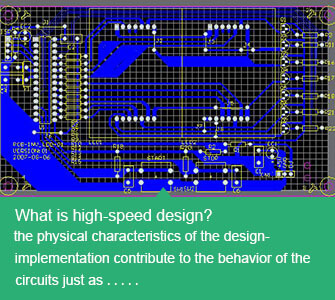
High speed PCB design is applied to devices that clock high frequencies, as that would require high-speed interfaces. The term high-speed, however, may be mistaken to refer to clock rate in this context, which is incorrect. Literally, high speed PCB design revolves around the edge rate.
So how can you distinguish a high-speed PCB design from a low-speed PCB design? Watch out for any of these characteristics:
Presence of high-speed interfaces including HDMI, Ethernet, Thunderbolt, USB, SATA, or any other high-speed data transfer interface.
Each circuit consists of other integrated circuits interconnected via high-speed interfaces like LVDS, DSI, DR3, etc.
Over the track, the signal propagation time does not go below 1/3 of the rise time for the signal.
The frequency of the digital signal is at least 50MHZ
The physical size of the PCB is small, and it's hard to locate individual components.
High Speed PCB Design Guidelines
As we've mentioned, high-speed PCB design is a rather challenging thing to do, especially regarding the keenness with which traces should be routed. There are some guidelines you should make use of to make a proper layout of any high speed PCB layout. These are:
Minimal use of vias
They are useful, yes, but the wrong design will result to signal reflection and attenuation. This is why you should have a maximum of two (2) vias for a single interconnect.
Length equalization
The two ends of a differential par need to be the same length. This ensures the receiver can adequately smoother common-mode noise. Ensure also that single-ended signals are routed in parallel in case of multiple signals to allow the signals to reach the destination at the same time.
Short trace lengths
Prefer shorter trace lengths to reduce attenuation. Attenuation occurs when the signals lose energy as a result of dielectric absorption.
Trace spacing
To minimize crosstalk, the trace spacing should be maintained at least five times the trace width (5W). More on this later under the rules.
High speed PCB design tips
The best way of learning how to design high speed PCBs is not only training but keeping on doing it till experience builds. The experience in turn makes everything run smoothly throughout the design process. If you haven't spent much time around high sped PCBs, you may not do it as fast and efficiently as an expert would do. There are however some tips you can leverage to your advantage, and design quality high-speed hoards.
These tips are also applied by professionals to simplify their work. Check them out below:
The first rule was that the trace lengths should be tuned to the near same length for high-speed design. With the modern CAD software available, you only have the option of controlling the entire length of the traces.
Since signal propagation time varies on the different layers, the overall length of the traces and the track sections on each layer should be aligned. This is only necessary where the tracks of a high-speed interface pass on several layers.
For better tuning accuracy, control the section lengths with an easy Excel or Google spreadsheet. This manual approach allows you to add the track lengths on the different layers, resulting in higher accuracy.
Impedance is another crucial aspect in high speed PCB design. Since you do not want to mess with a single impedance value, ensure that your PCB manufacturer is explicitly clear about their stack and tracks' parameters. If you cannot contact the manufacture, you should at least know how to read the datasheets and hardware design guides.
Even with the datasheets, you should realize that the actual impedance may vary slightly from what you calculate. Still, there are variances in material characteristics for components from different manufacturers.
When laying out design rules on your board, you should have selected the ideal manufacturer for your components and ensure all details are as per design. Some things you can learn directly from the manufacturer include what stack-up options they have for your desired number of layers, as well as the track lengths and their separating distances. This information is akin to obtaining the exact differential and single-ended impedances you need.
Some manufactured boards may require that you highlight the tracks for which you want a certain impedance.
Finally, even though it's going to increase the PCB manufacturing cost, you should instruct your manufacture to perform an impedance control procedure. This is one of the easiest ways of increasing the signal quality from the beginning of the high-speed PCB design.
High speed PCB design rules and challenges
In order for you to design and engineer a high-speed PCB, there are laid out design rules you need to adhere to for optimal efficiency. We shall address these directions and challenges next.
Trace length tuning
High-speed interfaces often require that trace length is tuned to synchronize signals before transmission through data lines, or else the board fails at the maximum frequency or worse still, fails to work at all.
Generally, the higher the interface frequency is the higher the length matching demands. You should thus tune the trace length for all parallel interfaces. As you tune the trace lengths, ensure you get the right lengths for a given group of signals.
Impedance
When designing a high-speed PCB, pay close attention to both single-ended and differential impedances, (Zo, and Zdiff respectively). Other common types of impedance include Odd Mode, Common Mode, and Even Mode.
Using a wrong impedance will result to signal reflections inside the track. This in effect, decreases the working frequency, generates unwanted EMIs, and leads to the loss of signal quality. To avoid all that, use the right impedance.
Track shape
Even though the standard requirement for track shapes should be round and with smooth corners and no sharp bends. This would be generally time-consuming, but you must avoid making 90-degree bends. However, you have the option of bending the tracks by 45 degrees. A sharper angle than this would produce reflections and impedance changes, as well as higher values for uncoupled length in differential pairs.
Termination
Termination is the placement of a resistor between the tracks of a differential pair at the end of the line, near the receiver as much as possible. Termination helps rid of signal reflections thereby improving the quality of data transfer.
You should note that the resistor value should be equal or a little above the Zdiff in the case of differential pairs, failure to which over-termination will occur, degrading the signal quality.
You should also be keen on datasheets and hardware design guides for they can tell you if the IC you have has a termination resistor inside. Including an external resistor in such cases would lead to over-termination.
Grounding
Tracing a high-speed interface on one layer is something you do not really want to imagine. You need vias for you to move the trace over other layers.
When working with different layers, place GND vias as close to the layers as possible. This allows for uniform GND polygons potentials near the signal vias. This way, you'll be able to maintain the same GND reference all along the trace.
Components location
The length of the tracks is usually not very long. You should have this in mind when you start attaching components that are interconnected via high-speed interfaces so that you leave sufficient space for length tuning.
The high-speed interfaces should also not be placed close to the edge of the PCB, as this would affect the signal quality.
Placement of ground polygons on the layers close to the signal layers
The general rule here is that all high-speed interfaces' tracks should be routed over a solid GND plane.
So, to avoid gaining extra EMI, creating signal delays, interferences, integrity violation, and degrading the signal quality, never route the tracks over polygon-splits or polygon cutouts. Any track crossing a polygon-split should be corrected by placing ceramic stitching capacitors where the polygon splitting is, to minimize signal degradation.
Crosstalk
For any two neighboring tracks, a signal transmitted through one track causes an unwanted impact in the other track, a phenomenon known as crosstalk. Since the magnitude of the crosstalk depends on the length over which the tracks run parallel to each other, it is necessary to ensure that the gap between the pairs is at least five times the width of the track. You should ensure the same distance is maintained between the differential pair and any other track along the whole length of the former.
Conclusion for High Speed PCB Design
High speed PCB design may be one of the most challenging things to undertake regarding PCBs. It gets harder if the board size is small and locating the different components is difficult. This guide has covered the important guidelines, tips, and rules that will help simplify your high-speed PCB design.
Enjoy challenging your PCB design skills by diving into the high-speed PCB designs.
You may have interest in our PCB design, PCB assembly, circuit board and electronic manufacturing services. Take us as your top PCB manufacturer!
If you have any comments or suggestions about this post, please leave a reply here
Previous article:Aluminum PCB substrate the same as the printed circuit board


