General, quoting & support.
Add: Building E, No.58, Nanchang Road, Xixiang , Baoan District Shenzhen City, Guangdong, China
Tel : 0755-27348887
Fax : 0755-27349876
E-mail : svc@pcbastore.com
A Comprehensive Guide to BGA Assembly in SMT PCB Manufacturing: Step-by-Step Breakdown
PCBA Store / 2026-02-19
Contents [hide]

Ball Grid Array (BGA) assembly forms a key part of today's Surface Mount Technology (SMT) PCB manufacturing. It helps fit high-density, high-performing parts into small electronic devices. BGAs differ from old leaded parts. They use a grid of solder balls on the bottom to link to PCB pads. This setup provides better heat handling, clear signals, and space savings. Yet, putting them together needs careful work, tight process checks, and modern inspection methods. These ensure solid links. In this guide, we cover the full BGA assembly steps in SMT PCB manufacturing. We start from early setup to final checks. We point out main steps, common rules, and good habits to skip flaws. At PCBA Store, we focus on one-stop PCB assembly as a leading PCBA supplier. We give high-quality PCB Assembly BGA and SMT Circuit Boards solutions made for your needs.
Pre-Production Preparation: PCB and BGA Component Readiness
Before starting BGA assembly, a full setup of the PCB and BGA parts is a must. This phase sets the base for clean soldering and lasting strength. Even small dirt or rough handling can cause problems. These include weak joints, gaps, or part breakdowns.
PCB Preparation
PCBs for BGA assembly must hit strict quality marks. They support exact part placement and soldering. Main steps cover:
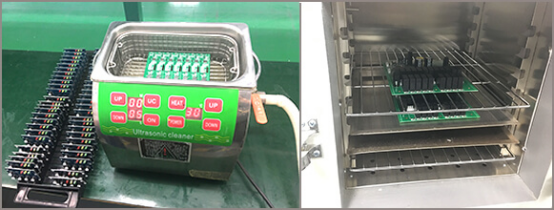
· Cleaning: Use ultrasonic cleaners to clear dust, flux leftovers, or oils from PCB surfaces. Dirt can block solder paste from sticking. It may create soft joints. After cleaning, make sure PCBs are dry fully. This stops water-based flaws in reflow soldering.
· Moisture Control: PCBs take in water over time. That can lead to “popcorning”. This means splitting or breaking when hit with high reflow heat. Preheat PCBs at 120–150°C for 4–6 hours. This pulls out trapped water. Follow IPC-J-STD-020 rules for moisture/reflow sensitivity.
· Storage: Store ready PCBs in a set space. Keep the temperature at 20–25°C. Hold relative humidity (RH) under 50%. Use anti-static packs or vacuum-sealed bags. They guard against dust, electrostatic discharge (ESD), and water. Mark each group with make dates and storage details. This aids tracking.

BGA Component Preparation
BGA parts are fragile and open to the surroundings. So, right handling matters a lot:
· Inspection: Before putting together, look over BGA parts for body harm. Examples include cracked packs or solder balls. Also check for dirt like flux on balls. Use a stereomicroscope with 10–20x zoom. It checks if solder balls match in shape. Balls need to be round, same size, and without rust.
· Moisture Management: Like PCBs, BGAs get rated by moisture sensitivity levels (MSLs) under IPC-J-STD-033. If kept past shelf time, bake BGAs at 125°C (±5°C) for 8–12 hours. The time depends on MSL. This removes water. Do not bake parts more than three times. It can harm pack strength.
· ESD Protection: BGA parts can suffer ESD harm. That leads to the inside circuit failing. Handle with ESD-safe tools. These include grounded tweezers and anti-static mats. Make sure workers wear ESD wristbands or heel straps.
Solder Paste Application: The Foundation of Reliable BGA Joints
Solder paste acts as the “glue” that joins BGA solder balls to PCB pads. So, picking it and putting it on affects joint power and steadiness right away. This step calls for care. It makes sure the right paste amount goes on evenly. Too small an amount makes weak joints. Too much can cause short paths or links.
Solder Paste Selection
For BGA assembly, lead-free solder paste is the common choice. It follows RoHS rules. The usual mix is 99.7% tin (Sn) plus 0.3% copper (Cu). Other mixes like Sn-Ag-Cu or Sn-Bi-Ag fit certain uses. For example, low-heat reflow for warm-sensitive parts. When choosing solder paste, think about the main traits:
· Viscosity: Good viscosity sits at 800,000–1,200,000 cP (centipoise) for stencil printing. High viscosity leads to bumpy spreading. Low causes paste to sag before reflow.
· Particle Size: Pick solder powder at 25–45 μm for BGAs with pad spaces ≤ 0.5 mm. Small bits help paste move through tight stencil holes.
· Flux Content: Flux fills 8–12% of the solder paste. It clears rust from pads and balls. It also stops new rust in reflow. Opt for no-clean flux in most cases. It skips after-soldering cleaning. That can hurt BGAs.
Stencil Printing: The Preferred Application Method
Stencil printing stands as the best way to put solder paste on BGA pads. The steps include:
· Stencil Design: Pick a stainless steel stencil. Its holes match BGA pad sizes. Usually, they are 80–90% of the pad size to stop linking. Stencil thickness goes from 0.12 to 0.15 mm for BGAs. This gives enough paste amount.
· Printing Parameters: Set squeegee speed at 20–30 mm/s. Use a pressure of 10–15 N. Set separation speed at 1–3 mm/s. These make even paste layers. A full auto stencil printer keeps things steady. This works well in big production runs.
· Paste Inspection: After printing, use a Solder Paste Inspection (SPI) system. It checks the paste amount, height, and evenness. SPI spots flaws like no paste, extra paste, or off-center spots early. This cuts the work later.

BGA Placement: Precision is Non-Negotiable
BGA placement needs accuracy under a millimeter. It lines up each solder ball with its PCB pad match. Even small offsets of 0.1 mm or more can lead to open paths, weak joints, or links. Auto pick-and-place machines are vital for this care. They suit high-density BGAs especially.
Equipment and Setup
· Pick-and-Place Machines: Use modern SMT pick-and-place systems. Examples include Juki RS-1 and Yamaha YSM40. They have vision-matching features. These offer placement accuracy of ±0.01 mm. Repeatability hits ±0.005 mm. This keeps alignment steady.
· Fiducial Markers: Add fiducial markers to PCB corners and near BGA pads. These are small, clear dots. The machine's vision setup uses them to adjust the PCB spot. It fixes small board bends or handling slips.
· Component Calibration: Before placement, adjust the machine for each BGA part. This means scanning the part's sizes. Like package size and solder ball space. Then, set the pick-up nozzle size. This avoids harm to the part or balls.
Placement Process
1. Component Pick-Up: The machine uses a vacuum nozzle to lift the BGA from tape-and-reel or a tray. Match nozzle size to BGA package. For a 10×10 mm BGA, use a 5 mm nozzle. This gives a safe, level lift.
2. Vision Alignment: Move the BGA under a high-detail camera. It takes pictures of the solder ball grid. The machine matches these to a digital PCB pad model. It figures any needed changes for the line-up.
3. Placement: Lower the BGA onto paste-covered pads at a set speed of 1–2 mm/s. Use a pressure of 5–10 N. Release the vacuum. Pull back the nozzle. This leaves the BGA set.
Reflow Soldering: Creating Strong Metallurgical Bonds
Reflow soldering heats the built PCB. It melts the solder paste. This makes lasting bonds between BGA solder balls and PCB pads. This step needs a managed heat path. It avoids part harm and gives the best joint quality.
The Reflow Temperature Profile
A usual reflow path has four clear zones. Each has a set heat range and goal. Tailor the path to the solder paste type. Like lead-free or leaded. Also fit component heat sense:
Zone | Temperature Range | Duration | Key Purpose | Impact on Solder Joint Quality |
Preheating Zone | 100–150°C | 60–90 seconds | Gradually raise PCB temperature to prevent thermal shock. | Prevents component warping, PCB delamination, and solder paste drying. |
Soaking Zone | 150–180°C | 60–120 seconds | Activate flux (remove oxidation) and ensure uniform heating. | Minimizes temperature variations across the PCB; ensures flux cleans pads/balls. |
Reflow Zone | 235–250°C (peak) | 30–60 seconds | Melt solder paste and form metallurgical bonds. | Critical for creating strong, void-free joints; peak temperature must exceed solder’s melting point (217°C for Sn-Cu paste). |
Cooling Zone | 250°C → 100°C | 60–90 seconds | Rapidly cool the PCB to solidify solder joints. | Prevents excessive intermetallic compound (IMC) formation (IMC thickness ≤ 5 μm is ideal); ensures joint integrity. |
Profile Optimization Tips
· Ramp Rate: In the preheating zone, heat rise should be 1–3°C per second. Quick rise brings thermal shock. Slow rise dries flux before reflow.
· Peak Temperature: For lead-free solder (Sn-Cu), peak heat should be 18–33°C over melting point (217°C). Over 250°C harms BGAs. Like pack cracks. Under 235°C leaves solder unmelted.
· Time Above Liquidus (TAL): Time over melting point (217°C) should be 30–60 seconds. Too short makes cold joints. Too long causes solder balls or pad lifts.
Post-Reflow Cleaning
After reflow, some flux may stay near the BGA. For no-clean flux, cleaning is not always needed. But for high-trust uses like car or medical, use isopropyl alcohol (IPA) and a soft brush. Gently clear flux leftovers. Skip strong cleaners like acetone. They can hurt BGA packs.
Inspection and Testing: Ensuring Reliability
BGA solder joints hide under the part. So, basic sight checks fall short. Mix of modern inspection ways and electric tests is needed. They find hidden flaws. Like gaps, open paths, or head-in-pillow issues. They also make sure the PCB works right.
Key Inspection Methods for BGA Assemblies
Different methods aim at setting flaw types. So, a layered plan works best:
Inspection Method | Description | Defects Detected |
Visual/Optical Inspection | Use a stereomicroscope (20–50x magnification) to check BGA placement and external defects. | Misalignment, component damage, solder bridging (between exposed pads), flux residues. |
Automated Optical Inspection (AOI) | Use high-resolution cameras and image analysis to inspect solder joints and placement. | Missing components, misalignment, excessive flux, solder balling. |
X-Ray Inspection | Use 2D or 3D X-ray systems to visualize hidden solder joints under the BGA. | Voids (≤ 25% of joint area is acceptable), open circuits, shorts, head-in-pillow defects, insufficient solder. |
Acoustic Microscopy | Use soundwaves to detect internal defects in BGA packages or solder joints. | Delamination (package-pad separation), voids in the BGA substrate, cracked solder joints. |
Infrared Thermography | Capture heat signatures of the BGA during operation to detect thermal anomalies. | Poor thermal connections (e.g., cold joints), component overheating. |
Electrical and Functional Testing
Checks alone do not cut it. Electric testing proves the BGA assembly does its job:
· In-Circuit Testing (ICT): Uses a bed-of-nails fixture to test single parts and links. ICT finds open paths, shorts, wrong part values, and bad solder joints.
· Flying Probe Testing: A fixture-free choice to ICT. It uses moving probes for BGA links. Great for test models or small runs. No custom fixtures needed.
· Functional Testing: Copies real use conditions. Like voltage, current, signal input. It checks overall PCB work. For BGA setups, this tests signal clarity, heat handling, and power flow.
· Solder Paste Inspection (SPI): Done before reflow, SPI looks at paste amount and evenness. It stops after-solder flaws. This key early test cuts fix costs.
Quality Metrics for BGA Assemblies
To gauge success, follow main quality measures:
· First-Pass Yield (FPY): Percent of PCBs passing all tests first time. High FPY at ≥ 99% shows strong process watch.
· Void Rate: Percent of joints with gaps over 25% of the area. Such gaps cut heat and electric flow.
· Defect Density: Flaws per 1,000 BGA joints. Aim for ≤ 0.1 flaws per 1,000 in trust-heavy uses.
Conclusion
BGA assembly in SMT PCB manufacturing is a careful, multi-step process. It needs good setup, exact placement, managed reflow, and strict testing. By sticking to common rules, fine-tuning settings, and using modern check tools, makers can build steady BGA setups for tough uses. At PCBA Store, we stand out as a manufacturer, supplier, and factory. We provide full one-stop PCB assembly solutions that hit top performance and strength marks.
Call to Action
Ready to elevate your PCB Assembly BGA projects? As a dedicated manufacturer, supplier, and factory, we at PCBA Store offer tailored SMT Circuit Boards and PCB Assembly services with no MOQ, fast turnarounds, and ISO9001-certified quality. Get an instant quote today at https://www.pcbastore.com/online_quote.html, explore our capabilities at https://www.pcbastore.com/pcb-capabilities.html, or learn why businesses choose us at https://www.pcbastore.com/why-us.html. Contact us now to streamline your production and achieve superior results.


