General, quoting & support.
Add: Building E, No.58, Nanchang Road, Xixiang , Baoan District Shenzhen City, Guangdong, China
Tel : 0755-27348887
Fax : 0755-27349876
E-mail : svc@pcbastore.com
Flying Probe Test: All You Need to Know
Simon / 2021-09-11
Contents [hide]
We are all aware of the Printed Circuit Boards and their impact on the core electronic products' efficiency. They typically come with a hardened green colored board that mostly appears in all electronic devices when it's opened. PCBs are completely loaded with various types of electronic components such as capacitors, inductors, resistors, chokes, ICs, transformers, connectors, jumpers, and several other stuff.

To ensure the proper functioning of the circuit boards, it's very crucial to make sure that the PCB along with its components aren't faulty. There shouldn't be any defects and the connection must be properly laid out.
It becomes necessary to check whether all the components along with the PCB itself are working fine. Some specific tests broadly termed as the 'Electrical Performance Test' are conducted by the PCB manufacturers. These tests are broadly classified as in-circuit tests and flying probe test.
With these tests, one can ensure that both the stuffed as well as bare PCBs which leave the manufacturing unit are comprehensively tested under various electrical parameters. These parameters include voltage, resistance, capacitance, current, short and open circuit.
What is a flying probe test?
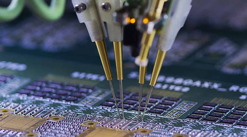
Flying probe testing, as its name goes, utilizes test probes that move from one test probe to another by flying. In this method, no custom fixture is needed which implies that it could also be referred to as a fixtureless in-circuit testing when used over an assembled PCB. As a result, it becomes highly cost-effective for low to mid-range production.
The flying prober originally evolved to be used simply for bare board testing. Today, it is hailed as the regulation for bare-board testing that includes testing for opens and shorts in between the copper conductors. The primary electrical parameter that is evaluated here is the lying resistance in between two nodes or points.
Gradually, the flying probe test has evolved to measure the induction and capacitance along with resistance. This makes them beneficial for the use of PCB assembling also. These tests are armed with a dedicated camera for inspecting the polarity of components. It is now considered as a more attractive firm of testing, particularly with the ongoing maturing trend of electronics.
What is an in-circuit test?
The in-circuit test, commonly referred to as ICT, is a strong tool of PCB testing. It uses a later of nails in-circuit equipment, it becomes easier to have access to the circuit nodes present on the board for measuring the performance of various components.
Since most faults of the PCB stem from the process of manufacturing and they typically constitute an open circuit, short circuit, or wrong components, this kind of testing is effective in catching most of the issues with the board. One can easily check these with the aid of sample measurements, capacitance, resistance, and also inductance lying in between two nodes on the board.
One of the major reasons for IC failing is the static damage which typically showcases itself in the places where in-circuit is close to the connecting outside world. Such failures can be effortlessly detected through the in-circuit testing technique.
Some in-circuit testers can also test several functionalities of integrated circuits. As a result, it instils better confidence in the structure and chances of operation on the PCB. Even though an in-circuit test offers no testing on the board functionality, when the assembling and designing are done correctly, it should work fine.
Flying probe testing vs in-circuit testing during PCB assembly
It can be an overwhelming task to decide the best method for testing a PCB. There are tons of factors that should be taken into consideration for this. But there are two main kinds of strategies for testing: the flying probe test and the in-circuit test.
Now the question is which of these two automation tests is the best? Will it be better if one opts for a combination of both these testing techniques to achieve the desired level of coverage? Let's take a look at the two options with their strengths and weaknesses to determine the best option.
Product design
In-circuit testing comprises individual probes devised for making contact with the test points on an assembled circuit boards. This helps in checking for any assembly defects along with the functionality of the board. Every net of the board comes with a test point on it for testing which makes it possible for a test fixture to contain loads of probes.
Flying probe testing is an automatic system that controls two to six problems that fly all around the printed circuit board for contacting test points in both the upper and the lower layers of the board. In this method, there is no need for a test fixture since the probes themselves move to the particular test point locations. So, from this prospect, the flying probe test is the winner.
Lead development time
The in-circuit center takes a lot of time in creating test fixtures. Every test fixture prepared can be created only when the PCB layout has been finalized. Moreover, if any revision is required in the layout, will only result in a change in the test fixture and in some instances, may require a completely new fixture being required. Therefore, the time required for lead development may increase.
One of the most important benefits of the flying prober is that has a relatively lower cost and takes less development time. Since it can be set up very quickly, it is often used for an additional level of test validation at a very low impact on the whole testing and assembling process.
Expected volumes
In-circuit testing is a board testing system containing numerous probes called a bed of nails. The ICT probes can make parallel contact with every test point for the electrical testing of circuits. It is time-consuming and cannot handle a large volume within a brief time.
Flying probe tests are meant to handle a large amount of PCB layout revision as no fixture is required for modification. The whole thing to be taken care of is an adjustment of the program. It can also take care of larger boards compared to the ICT system which makes it a popular choice for large backplane testing.
Cost
The cost incurred in programming is based on the complicated of the assembly, but this is typically the same for both the test solutions. But when concerning the other charges related to the test, there are certain key differences to be aware of:
The cost of fixture of flying probe test is typically zero whereas, it can run to thousands in case of ICT. The development time for flying probes is generally a week at the most whereas ICT can take about six weeks including both manufactures as well as programming. This means that ICT may be costlier compared to a flying prober.
How flying probe testing works?
For smooth testing of circuit board assembly in the flying probe test, it is important to create a full-on FPT test. This program is typically created in offline mode and every FPT offers a Test Program Generation Application running on a computer. With the generation of the test program, it can be loaded into the flying probe tester. The circuit board assembly that has to be tested is then put on the conveyor belt. This allows it to go into the testing area where the probes are located.
With the test program running, the probes which remain under the program's control will be able to contact the pads. Now the tester applies electrical test signals along with the power to the probe zones for making the precise measurements.
These measurements are processed within the tester to assess whether the circuit portion inside the probes is able to give the desired results. In this way, the flying probe detects whether there is any defect in the unit. The FPT then tries to isolate the parts among the testing probes in the interconnections to various other parts on the board.
Advantages of flying probe test
One of the most crucial benefits of a flying probe test is that the upfront cost is comparatively lower than ICT. Another factor is that a flying probe offers 99 percent accuracy which means that the user would have no problem with the end-product.
The next advantage of a flying prober is that no design decision or testing is required. This includes its ability to testing double-sided boards. It can test a single side at any given time without any issues. This is a sure contrast to an in-circuit testing method where the user has to design the PCB for the testing fixtures for accessing the various components.
Disadvantages of flying probe test
As it goes with most other tests, FTP cannot power up a circuit which implies that a user cannot have a realistic view of the product. Moreover, it cannot inspect ball grid array since the flying prober needs access points for connecting to the components.
Conclusion
It goes without saying that PCB testing is very tricky and based on the complexity of the project. A flying probe is definitely the most effective and efficient PCB testing technique and it is used in most manufacturing applications around the world.
Previous article:What is PCB Panelization


