General, quoting & support.
Add: Building E, No.58, Nanchang Road, Xixiang , Baoan District Shenzhen City, Guangdong, China
Tel : 0755-27348887
Fax : 0755-27349876
E-mail : svc@pcbastore.com

What Is Solder Paste and How Does It Improve SMT Assembly Quality?
PCBA Store / 2026-07-31
Contents [hide]
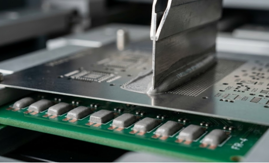
Understanding Solder Paste in Surface Mount Technology (SMT)
Definition and Composition of Solder Paste
Solder paste works as a semi-solid mixture. It blends fine solder alloy powder with flux. This mixture forms the main bonding material used for soldering circuit boards. The flux part cleans oxidation off metal surfaces. This cleaning ensures good wetting during the reflow stage. The alloy mixture usually contains tin combined with silver or copper. This specific metal mix decides the melting point, wetting ability, joint strength, and electrical flow. These features directly affect the reliability of the solder joint. They also determine the long-term life of the finished PCB SMT assembly. In highly reliable electronics like aerospace systems, a steady paste mixture is very important. Any change can cause cold solder joints. These bad joints will harm the electrical performance.
The Function of Solder Paste in the SMT Process
During PCB SMT production, solder paste does two main jobs. First, it works as a short-term glue. This glue holds parts in their correct spots before reflow heating. After heating, the tiny solder pieces melt. They build strong metal bonds between the part leads and the board pads. A PCB stencil ensures workers apply this paste layer exactly across all pads. This action lowers electrical resistance and mechanical strain. It also makes sure the solder joints form evenly. Modern printing machines use vision alignment cameras. These cameras make sure every paste drop lands perfectly. This exact placement is highly important for tiny parts like BGAs and QFNs.
The Role of the Paste Layer in PCB Assembly
The paste layer PCB setup has a huge impact on joint quality. An even thickness makes sure strong connections happen across all pads. On the other hand, uneven spots can create bad defects. Too much paste might cause bridges between pads sitting next to each other. This extra metal leads to short circuits. Too little paste can create open or weak connections. Because of this, keeping the solder paste layer perfectly even is necessary. It helps factories reach high success rates during SMT assembly jobs.
Paste Thickness | Common Defect Type | Resulting Issue |
Too Thick | Bridging | Short Circuits |
Too Thin | Insufficient Joint | Open Connections |
Uneven | Voiding/Stress | Mechanical Failure |
How PCB Stencils Enable Accurate Solder Paste Application
Laser-Cut Stencils
A circuit board stencil—usually built from stainless steel—gets cut by lasers to match pad designs exactly. This tool makes sure the solder paste goes down accurately before machines place the parts. Laser cutting creates very smooth hole walls. These smooth walls let the paste release cleanly. This clean release works well even for tiny parts found in phones or smart watches. For high-tech uses like microelectronics stencil printing, carefully adjusted laser holes guarantee precise paste transfer at very small sizes.
Electroformed Stencils
Factories make electroformed stencils using special nickel shaping methods. These methods build extremely smooth hole walls. They also provide excellent paste transfer results. These stencils work perfectly for crowded PCBs. On these boards, the space between parts is very small. The great surface finish lets the stencil drop the same amount of paste over thousands of uses. The stencil will not wear out quickly.
Common Issues Related to Solder Paste Application in SMT Lines
Insufficient or Excessive Paste Deposition
The wrong stencil thickness can ruin the print. Old squeegee blades also cause bad printing results. These mistakes lead to broken joints or metal bridges after the heating process. Such errors lower the final assembly quality. They might also force workers to fix the boards or throw them away.
Misalignment Between Stencil and PCB Pads
Even a tiny shift between the stencil holes and the board pads causes major problems. It can create bridges or leave connections completely empty after heating. Because of this risk, automatic camera alignment systems are necessary. They keep the position perfectly accurate while the machine prints.
Handling Problems After Printing: Drying or Contamination of Printed Paste
Leaving printed boards out in the open for too long is a bad idea. The liquid parts in the flux will dry up. This drying makes the paste less sticky. It also changes how the paste spreads during the heating stage. When this happens, the metal might not wet the pads properly. It can also leave the joints open after reflow. Learning how to solder a circuit board properly includes managing the paste drying time.
Component Placement Errors
Bad part placement lowers the grip between the parts and the wet paste. Dirt on the pad surfaces does the same thing. When the board goes into the oven, these loose parts might slide or stand up on one end. This standing issue is called tombstoning. These crooked parts will break the circuit connections.

How Manufacturers Control Solder Paste Quality in SMT Production
SPI Inspection Ensures Printing Quality
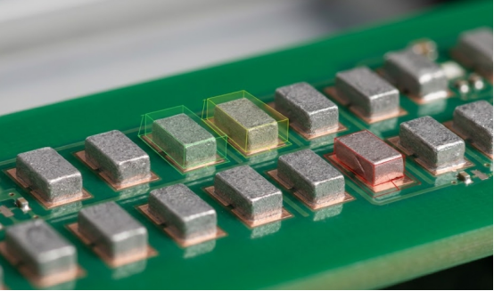
Solder Paste Inspection (SPI) machines check the paste right after printing. They measure the volume, height, flat area, and exact position. These scanners find missing paste drops or shifted prints very early. Workers can remove these bad boards before the placement and heating steps start.
Viscosity Monitoring Maintains Paste Performance
Paste thickness, or viscosity, decides how easily it pushes through the stencil holes. Regular checks make sure the flow stays inside the best range. Changes in thickness cause problems. Too thin paste will slump over the pads. Too thick paste will leave empty spots. Keeping the right thickness stops bridges and empty bubbles during the assembly process. This control is a key part of successful soldering on PCB projects.
Proper Storage Management Preserves Material Stability
Solder paste needs careful temperature control to keep the flux working well and stop rust. Factories usually keep it in a fridge between 0°C and 10°C. Workers must let the paste warm up to room heat before they open the jars. Bad storage creates water drops inside the containers. This extra water ruins the material quality over time.
Printing Accuracy Improves Assembly Reliability
Exact matching between the PCB stencil and the board pads is important. It guarantees the paste lands in the right spot for every pad design. This includes very small ICs like BGAs or QFNs placed under a solder mask layer. Changing the blade pressure and the printing speed helps the paste transfer perfectly. It also stops the paste from smudging around the outside of the pads.
FAQ:
Q: What is solder paste used for in SMT?
A: Solder paste works as a temporary adhesive and electrical connection material in SMT assembly. During reflow heating, the metal particles melt and form strong joints between component leads and PCB pads.
Q: Why is stencil quality important for applying solder paste?
A: A high-quality PCB stencil ensures accurate paste placement on each pad. Poor stencil alignment or design can cause solder bridges, missing solder, and lower PCBA reliability.
Q: What happens if too much solder paste is applied?
A: Excess solder paste can create solder bridges between nearby component leads, causing short circuits. Proper printing control helps reduce defects, rework costs, and material waste.
Q: How should unused solder paste be stored?
A: Unused solder paste should be sealed and stored under controlled conditions, usually in refrigeration. Before use, it should return gradually to room temperature to prevent moisture issues.
Q: What are step stencils used for?
A: Step stencils have different thickness areas on one metal sheet, allowing different components to receive the right solder volume. They improve printing accuracy for complex PCBs with mixed component sizes.



