General, quoting & support.
Add: Building E, No.58, Nanchang Road, Xixiang , Baoan District Shenzhen City, Guangdong, China
Tel : 0755-27348887
Fax : 0755-27349876
E-mail : svc@pcbastore.com
2021 Detail Guide for Bluetooth Circuit
Simon / 2021-05-30
Contents [hide]
The advancement in technology has been a game-changer in almost every niche. In fact, you can all attest that this technology has made life to be more comfortable and accessible. Bluetooth technology for instance is one of the advancements that have seemingly transformed the communication sector. Do you remember when we used cables and wires in fostering communication among or between devices? All thanks to Bluetooth that has introduced wireless technology. In other words, Bluetooth technology is an upgrade of the initially infrared technology that only connected two gadgets same time; thus it is a huge issue. Using Bluetooth, therefore, help connect several devices and share data at the same time. This is made possible by the Bluetooth circuit board as we shall learn from this piece.

What is the Bluetooth Circuit?
A Bluetooth circuit is considered the ground of the Bluetooth and comprise of various components, including capacitors, integrated circuits, and power source. The Bluetooth circuit also possesses backed wired-in audio, Bluetooth modules, among others. The integrated circuit contains a voltage regulator and a charger. The next is the Bluetooth model which is a component that comprises the details on the settings and configuration.
The Bluetooth circuit has a connection that ranges at 2.4 GHz. When connecting devices, there will be the main device which is perceived to be the master device. The other connected device is commonly known as the slave.
Components of a Bluetooth Circuit Board
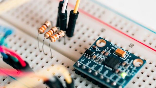
A Bluetooth circuit board has various vital components such as an antenna that aid in receiving and sending information. A complete Bluetooth circuitry also possesses a minimum of two inductors whose task is adjusting the antenna's impedance to strengthen the overall performance. There is also a module containing up to 4 IO pins, which are Enabled, power supply, State, and communication options. The Bluetooth circuit board still includes several diodes, resistors, and capacitors.
What's more? The Bluetooth circuit board possesses other components like the voltage, crystal-based clock, chips, and regulators. Due to these overwhelming and sensitive components, the Bluetooth circuit board demands careful handling while assembling. This is a must considering the antennae for its ideal functioning. With that in mind, all these are what make the Bluetooth circuitry board. Just remember that you can get these circuit boards from Bluetooth-enabled gadgets such as wireless earphones and headsets, cordless mouse and keyboards, among others.
Bluetooth Circuit Board Design Guidelines
The PCB boards employing Bluetooth technology are often challenging to design. Without proper design, therefore, means poor device and the overall performance. In simple terms, a poor Bluetooth circuit can be an issue with lost data, interference, and poor signal integrity. Despite that, some guidelines help you design these Bluetooth circuit boards easily. The outline below is to give you some rules and guidelines to ponder when selecting a Bluetooth technology to implement for a particular application. Different applications employing Bluetooth technology encompass:
Eddystone frames utilized in firm sensing applications
Remote peripheral gadgets like computer keyboards/mice or video game controllers
Wireless consumer electronics such as printers, cameras, and phones
Beacons employed in shopping malls
Audio/stereo and headset products
Home automation systems
All these applications employ similar Bluetooth technology; however, the implementation is somewhat different and relies on the type of connection. For that reason, design engineers must embrace the common principles to optimize the device effectiveness and the overall integrity signal.
Basically, Bluetooth technology is a fast wireless option; however, it is not as fast as the Wi-Fi wireless choice. The main issue with Bluetooth is that it will perform poorly through walls, obstructions, and possess a poor range. Despite the challenges, it is yet an outstanding option with 5.0 being the recent upgrade of the 4.2. In most cases, it is a fairly low-power, secure, reliable, and popularly supported choice that can effortlessly be used on various peripherals.
So what should you do to minimize interference, optimize signal integrity, and reduce lost data packets? Below are some Bluetooth circuit design general rules and guidelines to always consider.
Consider certified modules
When linking Bluetooth to a device with limited resources, you must ponder a fully and pre-certified module. This is a plus, especially when fostering its creation and reducing time to the market. It can be costly but will save you energy and time in designing/placing antenna and EMI susceptibility.
Choose Bluetooth device wisely
Selecting the right Bluetooth gadget for the application is vital. You must also ensure that the antenna employed has the right size and is fully tuned. For a simple application like a beacon, you can use a cost-effective solution, low-power, and peripherals to save the board and the overall cost.
For Bluetooth applications such as data-exchanging or audio-streaming, you may require a significant Rx sensitivity, Tx power, and faster data rate.
In case you are considering an all-in-one option chip, you may ponder the chipsets having secondary or powerful processors that comprise of available SPI, PWM, DAC, UART, I2C, ADC, and GPIO pins.
Alternatively, if you are focusing on a heavy gadget requiring the RSSI reading, ensure that the RSSI monitor possesses enough dB resolution.
Detach high energy components and copper signals
If you are working on a board in a Bluetooth module or chipset, ensure the antenna section is fully free from components with high energy or copper signals. You also need to ensure that board layers and other sections are free of polygon and plane pours. In most cases, a layout guideline is given by the Bluetooth chipset manufacturers that you have to follow correctly when designing the PCB. When laying the antenna section manually, employ the ground plane correctly to foster great bandwidth at the input end. Besides, remember to create enough space for the turning compounds.
Ground stitching Vias is also critical to help keep undesired radiation at bay. If this radiation can get into the edge of the PCB, then it can penetrate and influence the near signals. If possible, be sure to optimize the shape of your board to the Bluetooth gadget and to the location of the antenna and avoid it getting to the edge as much as possible. When working on analog signals like audio, remember to detach the digital and analog ground planes. Another plus is protecting the electronics to reduce noise and avoid cross-coupling.
Understand the power supply
Power is a vital component that must be used carefully in all devices. You need to ensure that the rail taking power to the Bluetooth chip or module is very clean. You also need to use decoupling capacitors with the range (0.1uF and 10nF) and a bypass (1.0 uF) where applicable. It is also important to incorporate ferrite beads precisely on the power rail.
Use the right tools and analysis
When developing the antenna section, remember that the right tools are a plus. An example can be a network analyzer which helps tune and analyze the corresponding network.
Think of real-world obstructions
Different items can lead to de-tuning or obstruction when connecting Bluetooth to devices. These can be walls, metalized objects, water, computers WLAN technologies, wireless RF video, home phones, power source, and office lighting. Primarily, Bluetooth is highly susceptible to loss of signal even after pairing devices to close distance. In case there will be such a hindrance, you can consider a higher power gadget option and run on a slower Bluetooth speed to reduce the packet drop. Alternatively, when the device is inside an enclosed system, you will need to reduce the metallic material.
Understanding the Process of Bluetooth Circuit
Here is a quick step-by-step guide to help you understand the process of Bluetooth circuit better;
Pre-production
The board is created using your specified production information. The expert weighs your specification desires with the appliance you want to create.
Imaging inner layer
The imagine phase is what makes the circuit board traces. This process requires a photo device and UV light to share images.
Etching inner layer
At this stage, the aim is to get rid of any unwanted copper residues. After that, the dry film is removed to have the right copper circuitry that rhymes with the design of your PCB.
AOI
This process is to confirm that the inner layer has no unnecessary electronic residues and chemicals.
Lamination
An oxide layer is used on the inner side of the board to develop an insulating section. Copper foil is added to the lower and upper stack parts.
PCB drilling
Holes are created that are used as electrical contacts of the board.
Deposition of electroless copper
The holes are supplied with a thin layer of copper deposits. An ideal copper deposit is provided by PHT that helps to conceal the whole panels and the hole walls. The next thing is panel plating to achieve an outer layer with a thick copper deposit.
Imaging outer layer
This process appears the same as the internal layering phase. But in the outer phase drilling, the aim is to maintain the board circuitry and removing the dry film.
Graphic plating
At this stage, more dry film plating is done. The tin is applied just after copper is deposited to help avoid oxidation of the plated copper.
Etching outer layer
Here, the dry blue film is taken out. Next is getting rid of unnecessary copper residues. Last is removing tin residue to ensure a clean circuitry board.
This stage uses UV light and artwork to introduce some PCB components and get rid of other exposed parts. Next is curing other solder masks to make a top-notch finish.
Surface finish
This helps to maintain the copper circuitry exposed while offering clean solderable ground. The type of surface finish can be organic and metallic. The organic finish can be carbon and OSP printing while the metallic finish can be HASL, Immersion silver, ENEPIG/ENIG, and immersion tin.
Electrical testing
The board must be tested to ensure it is working as recommended and is free of defects.
Conclusion
One of the best ways to designing a great Bluetooth circuit board is to maintain professional standards, especially when assembling. Otherwise, not following the right approach will lead to the range, functionalities, and other essential features suffer.
Previous article:What is Black Printed Circuit Board


